Electrostatic suppressing element and production method thereof

A technology of electrostatic suppression and manufacturing method, applied in electrical components, resistor manufacturing, resistor components and other directions, can solve the problems of high product trigger voltage, electrode end face ablation, high production cost, low product cost and short response time , the effect of low leakage current

Inactive Publication Date: 2013-10-09
NANJING SART SCI & TECH DEV
View PDF8 Cites 10 Cited by
  • Summary
  • Abstract
  • Description
  • Claims
  • Application Information

AI Technical Summary

Problems solved by technology

However, the formation of the two opposite electrodes needs to involve photolithography and etching technology, and the production cost is high, and the length and width of the narrow gap between the electrodes are limited to a certain extent, which may easily cause the trigger voltage of the product to be too high and the dispersion is large, and the narrow Excessive current density between the gaps will also cause the electrode end face to be ablated

Method used


Image

  • Electrostatic suppressing element and production method thereof
  • Electrostatic suppressing element and production method thereof
  • Electrostatic suppressing element and production method thereof

Examples


Embodiment 1

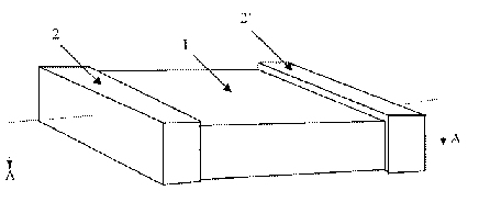
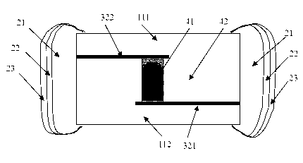
[0031] Such as figure 2 As shown, an electrostatic suppression component includes a ceramic substrate 1, a left external electrode 2 and a right external electrode 2', the left external electrode 2 and the right external electrode 2' are respectively located at both ends of the ceramic substrate 1, and the ceramic substrate 1 is protected by the upper layer 112, the second electrode layer 321, the via layer 42, the first electrode layer 322 and the lower protective layer 111, the via layer 42 is provided with an opening, and is filled with the pressure-sensitive ceramic functional phase 41, the via hole The upper and lower surfaces of the openings in the layer 42 are covered by printed electrode layers (322, 321). The printed electrode layers are alternately led out from both ends of the product, and each printed electrode layer is only connected to one external electrode. The thickness and shape of the printed electrode layer have no significant impact on product performance...

Embodiment 2

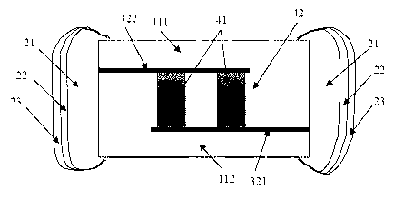
[0034] Such as image 3 As shown, an electrostatic suppression component includes a ceramic substrate 1, a left external electrode 2 and a right external electrode 2', the left external electrode 2 and the right external electrode 2' are respectively located at both ends of the ceramic substrate 1, and the ceramic substrate 1 is protected by the upper layer 112, the second electrode layer 321, the via layer 42, the first electrode layer 322 and the lower protective layer 111, the via layer 42 is provided with two openings, and both are filled with the pressure-sensitive ceramic functional phase 41, The upper and lower surfaces of the openings in the through-hole layer 42 are covered by printed electrode layers (322, 321), and the printed electrode layers are alternately drawn from both ends of the product, and each printed electrode layer is only connected to one external electrode .

[0035] Others are similar to Example 1.

Embodiment 3

[0037] Such as Figure 4 As shown, an electrostatic suppression component includes a ceramic substrate 1, a left external electrode 2 and a right external electrode 2', the left external electrode 2 and the right external electrode 2' are respectively located at both ends of the ceramic substrate 1, and the ceramic substrate 1 contains three layers The via layer 42 is composed of an upper protective layer 112 and a lower protective layer 111 located in the outermost layer. Each via layer 42 is provided with an opening and is filled with a pressure-sensitive ceramic functional phase 41. The via layer The upper and lower surfaces of the openings in 42 are covered by printed electrode layers, and the printed electrode layers on the upper and lower surfaces of the through-hole layer 42 are alternately arranged. The printed electrode layers are respectively drawn out from both ends of the product alternately. The side external electrodes are connected.

[0038] Others are similar ...


PUM

PropertyMeasurementUnit
The average particle sizeaaaaaaaaaa

Abstract

The invention relates to an electrostatic suppressing element and a production method thereof. The electrostatic suppressing element comprises a ceramic substrate (1), a left outer electrode (2) and a right outer electrode (2'), wherein the left outer electrode (2) and the right outer electrode (2') are arranged at two ends of the ceramic substrate (1) respectively, and the electrostatic suppressing element is characterized in that the ceramic substrate (1) consists of an upper protective layer (112), at least one through hole layer (42) and a lower protective layer (111), the through hole layer (42) is provided with at leas one through hole, the upper surface and the lower surface of the through hole are covered by a printing electrode layer, a voltage-sensitive ceramic functional phase (41) is filled in the through hole in the through hole layer (42), the printing electrode layer is alternately led out from two ends of a product, and each printing electrode layer is only electrically connected with the outer electrode on one side. The voltage of the electrostatic suppressing element is stable under an over-temperature condition, the response time is shortened, the weaknesses of a piezoresistor are overcome, and the electrostatic suppressing element has the characteristics of low electric capacity and small leaked current.

Description

technical field [0001] The invention relates to an electrostatic suppression element and a manufacturing method of the element, in particular to an electrostatic suppression element and method manufactured by using LTCC ceramic matrix stacking technology and pressure-sensitive ceramic material as a functional phase. Background technique [0002] All substances in nature are composed of atoms. Protons (positive charges) and electrons (negative charges) in atoms exist in every corner of our lives. Whenever two different materials come into contact with each other and separate, The so-called "triboelectric" effect occurs, and the subsequent transfer of charge to an object with a lower potential is called "electrostatic discharge (ESD)". It is difficult to completely eliminate static electricity in the process of static electricity protection, but we can take protective measures to minimize the generation and accumulation of static electricity, so the important issues facing des...

Claims


Application Information

Patent Timeline
IPC IPC(8): H01C7/10H01C1/142H01C17/00
Inventor 南式荣刘明龙
Owner NANJING SART SCI & TECH DEV
Why Eureka
Try Eureka