Luminescent device, display panel and manufacturing method of luminescent device and display panel

A light-emitting device and display panel technology, which is applied in the manufacture of semiconductor/solid-state devices, electric solid-state devices, semiconductor devices, etc., can solve the problems of unsuitable use, poor stability of light-emitting devices, high manufacturing costs, etc., to avoid agglomeration and oxidation, and stabilize Good sex and long life effect

Active Publication Date: 2013-10-09
TCL CHINA STAR OPTOELECTRONICS TECH CO LTD
View PDF5 Cites 37 Cited by
  • Summary
  • Abstract
  • Description
  • Claims
  • Application Information

AI Technical Summary

Problems solved by technology

[0006] However, the existing light-emitting devices have poor stability, are not suitable for the use of large currents, and have high manufacturing costs.

Method used


Image

  • Luminescent device, display panel and manufacturing method of luminescent device and display panel
  • Luminescent device, display panel and manufacturing method of luminescent device and display panel
  • Luminescent device, display panel and manufacturing method of luminescent device and display panel

Examples


Embodiment Construction

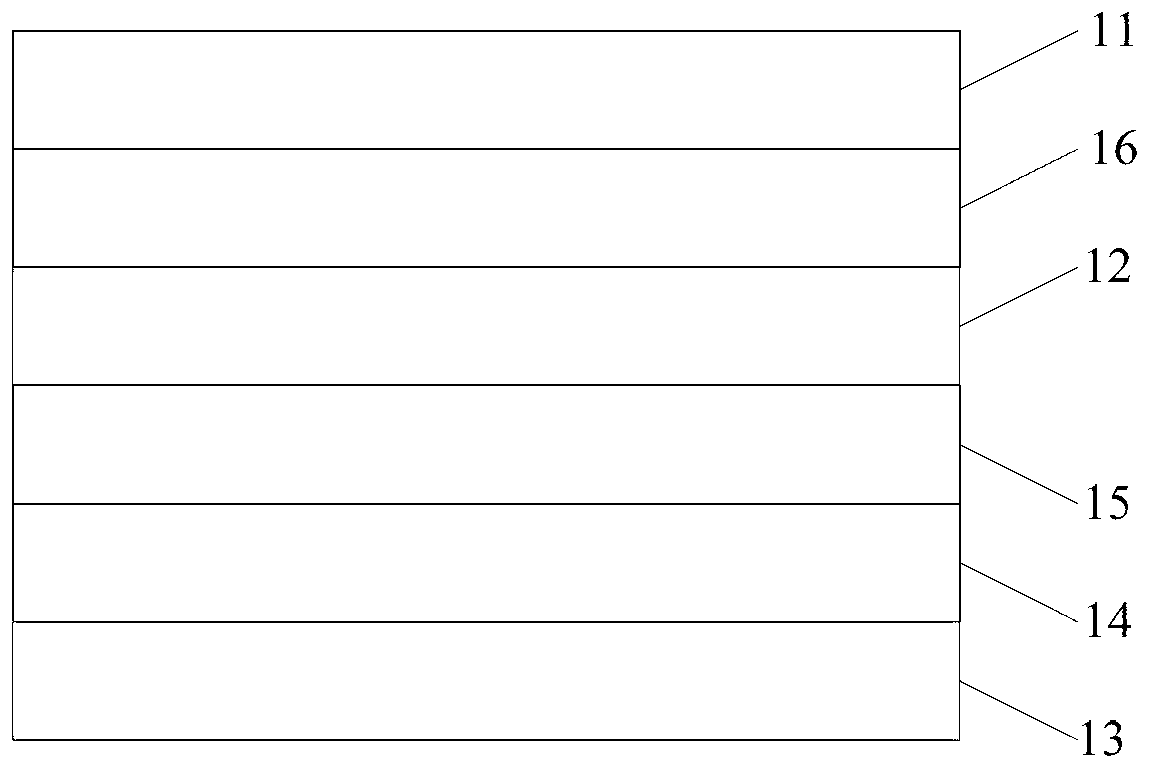
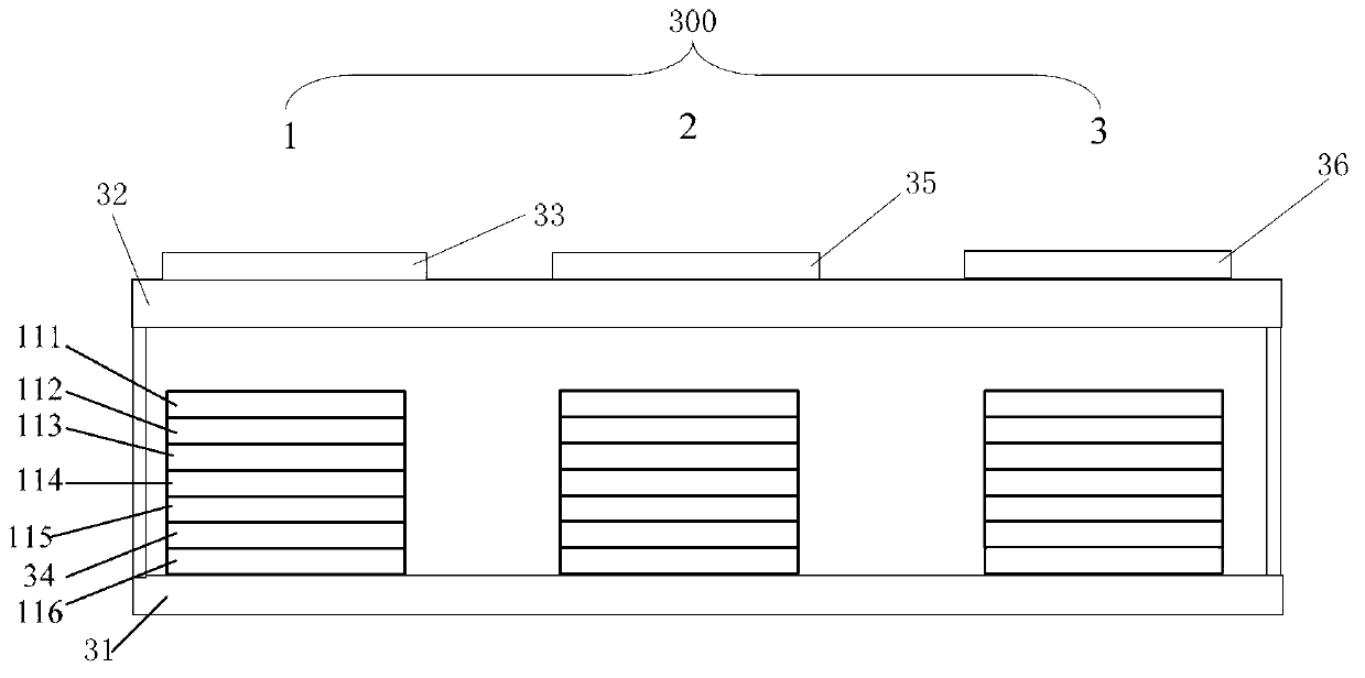
[0030] Semiconductor nanocrystals (Semiconductor Nanocrystals, NCs) refer to semiconductor nanocrystals with a size of 1-100nm. Since the size of semiconductor nanocrystals is smaller than the excitonic Bohr radius of their bulk materials, they exhibit strong quantum confinement effects, and the quasi-continuous energy bands evolve into discrete energy level structures similar to molecules, presenting new material properties. Also known as quantum dots (Quantum Dots, QDs). Due to excitation by external energy (photoluminescence, electroluminescence, cathodoluminescence, etc.), electrons transition from the ground state to the excited state. Electrons and holes in an excited state may form excitons. The electrons and holes recombine and eventually relax to the ground state. Excess energy is released through recombination and relaxation processes, possibly radiative recombination emitting photons. Therefore, the embodiment of the present invention utilizes this property of qu...


PUM


Abstract

The invention discloses a luminescent device, a display panel and a manufacturing method of the luminescent device and the display panel. The luminescent device comprises a cathode, an anode and a luminescent layer, wherein the cathode and the anode are arranged in an opposite mode, and the luminescent layer is arranged between the cathode and the anode and made of mixed materials of organic materials and quantum spot materials which emit white light. In this way, the stability and luminance of the luminescent device can be improved, and the luminescent device has the advantages of being ultrathin, transparent and easy to bend.

Description

technical field [0001] The invention relates to the field of display technology, in particular to a light emitting device, a display panel and a manufacturing method thereof. Background technique [0002] Diode is a semiconductor electronic component, while Organic Light-Emitting Diode (OLED) is a semiconductor electronic component that can emit light, also known as Organic Electroluminesence Display (OELD). OLED has the comprehensive advantages of cathode ray tube (CRT) and liquid crystal display (LCD), and is known as the flat panel display and third-generation display technology of the 21st century, and has become a major research hotspot in the world. [0003] The technical route for realizing the colorization of organic light-emitting diodes includes the following: [0004] 1. RGB three-color light emission, this method is only suitable for organic small molecule materials that are easy to sublimate, but the process is simple and mature, and the operation is easy; [...

Claims


Application Information

Patent Timeline
Patent Type & Authority Applications(China)
IPC IPC(8): H01L51/50H01L51/54H01L51/56H01L27/32
CPCH10K59/351H10K59/38H10K50/115H10K50/841H10K59/12H10K71/00
Inventor 刘亚伟王宜凡
Owner TCL CHINA STAR OPTOELECTRONICS TECH CO LTD
Why Eureka
Try Eureka