
GaSb-based mid-infrared circular spot output low divergence angle edge-emitting photonic crystal laser

A low divergence angle and photonic crystal technology, applied in the structure of optical waveguide semiconductors, etc., can solve the problems of reduced light confinement factor, large far-field emission angle, and small beam waist size of the fundamental mode beam, so as to reduce the far-field Divergence angle, increased light field area, high repeatability effect

Active Publication Date: 2015-07-29
INST OF SEMICONDUCTORS - CHINESE ACAD OF SCI
View PDF3 Cites 0 Cited by
  • Summary
  • Abstract
  • Description
  • Claims
  • Application Information

AI Technical Summary

Problems solved by technology

[0005] In prior art ridge strip waveguide lasers, the thickness of the active layer perpendicular to the P-N junction direction is ultra-thin, only tens of nanometers. The problem caused by the ultra-thin active layer is the reduction of the optical confinement factor, so in this direction The beam waist size of the fundamental mode beam that is similar to Gaussian distribution is small
And because in the semiconductor laser, the far-field divergence angle of the light beam is inversely proportional to the beam waist size produced by the active layer of the laser, so the very small beam waist produced in the active layer perpendicular to the P-N junction direction causes the far field in this direction. Large field emission angle

Method used


Image

  • GaSb-based mid-infrared circular spot output low divergence angle edge-emitting photonic crystal laser
  • GaSb-based mid-infrared circular spot output low divergence angle edge-emitting photonic crystal laser
  • GaSb-based mid-infrared circular spot output low divergence angle edge-emitting photonic crystal laser

Examples


Embodiment Construction

[0024] In order to make the object, technical solution and advantages of the present invention clearer, the present invention will be described in further detail below in conjunction with specific embodiments and with reference to the accompanying drawings.

[0025] It should be noted that, in the drawings or descriptions of the specification, similar or identical parts all use the same figure numbers. Implementations not shown or described in the accompanying drawings are forms known to those of ordinary skill in the art. Additionally, while illustrations of parameters including particular values ​​may be provided herein, it should be understood that the parameters need not be exactly equal to the corresponding values, but rather may approximate the corresponding values ​​within acceptable error margins or design constraints. In addition, the directional terms mentioned in the following embodiments, such as "upper", "lower", "front", "rear", "left", "right", etc., are only re...


PUM


Abstract

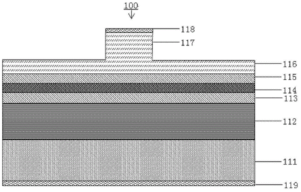
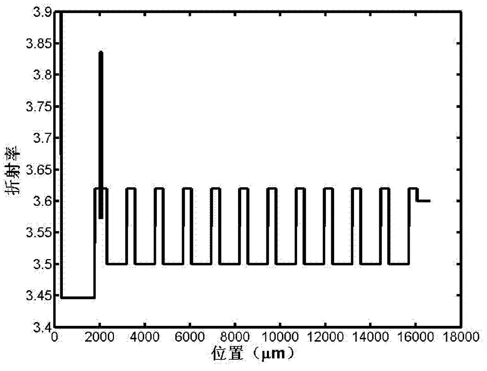
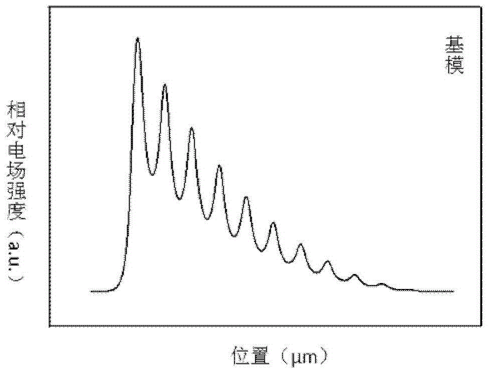
The invention provides a gallium stibino mid-infrared circular spot output low divergence angle edge photon emission crystal laser. The laser comprises an n type substrate, an n type electrode which is deposited on the reverse side of n type substrate, one-dimensional photonic crystals, a lower waveguide layer, an active layer, an upper waveguide layer, a p type cover layer, a ridge strip waveguide and a p type electrode, wherein the one-dimensional photonic crystals, the lower waveguide layer, the active layer, the upper waveguide layer, the p type cover layer, the ridge strip waveguide and the p type electrode are sequentially deposited on the front side of the n type substrate, and the ridge strip waveguide, the p type cover layer, the upper waveguide layer, the active layer, the lower waveguide layer, and the one-dimensional photonic crystals form a P-N knot. The alternating growth direction of the one-dimensional photonic crystals is perpendicular to the direction of the P-N knot, the direction of the ridge strip waveguide is parallel to the direction of the P-N knot, and the ridge strip waveguide and the one-dimensional photonic crystals form asymmetrical photonic crystal composite waveguides. The one-dimensional photonic crystals are imported to a ridge strip waveguide laser, and the mode perpendicular to the direction of the P-N knot can be regulated and controlled, so that the light field area of a ground mode is increased, and the far field divergence angle of the ground mode in the direction perpendicular to the P-N knot is reduced.

Description

technical field [0001] The invention relates to the technical field of semiconductor lasers, in particular to a gallium-antimony-based mid-infrared circular spot output low divergence angle edge-emitting photonic crystal laser. Background technique [0002] Compared with other lasers, semiconductor lasers have the advantages of high conversion efficiency, small size, light weight, high power, low threshold, and easy integration. Therefore, semiconductor lasers have been extensively studied by many research institutions. Semiconductor lasers operating in the mid-infrared band of 2-10 μm have shown great application potential in the fields of free-space optical communication, molecular spectroscopy, laser medical treatment, and infrared radar. Since the band gap of antimonide semiconductor materials can just cover this wavelength range, antimonide materials are the preferred materials for making mid-to-far infrared semiconductor lasers. [0003] From the first InGaAsSb / AlGaA...

Claims


Application Information

Patent Timeline
Patent Type & Authority Patents(China)
IPC IPC(8): H01S5/22
Inventor 郑婉华王海玲刘磊张建心张斯日古楞渠红伟张冶金
Owner INST OF SEMICONDUCTORS - CHINESE ACAD OF SCI
Learn More