Field programmable gate array chip layout method

A technology of chip layout and gate array, applied in the field of field programmable gate array chip layout, can solve the problems of unpredictable wiring stage interconnection, increased FPGA chip delay, and looseness, so as to improve the utilization rate of wiring resources and improve The success rate of wiring and the effect of reducing delay

Active Publication Date: 2013-10-23
SOI MICRO CO LTD
View PDF4 Cites 24 Cited by
  • Summary
  • Abstract
  • Description
  • Claims
  • Application Information

AI Technical Summary

Problems solved by technology

In most layout and routing tool software, the relationship between layout and routing is too loose. Usually, the interconnection lines used in the wiring stage cannot be predicted during layout, so the delay caused by the interconnection lines cannot be predicted, which eventually leads to FPGA chips. Increased delay
[0004] At present, the best solution to reduce the delay of FPGA chips is to perform layout and routing at the same time. However, when the layout and routing are performed at the same time, the running time of the placement and routing tool software will increase by more than ten times, which seriously affects the placement and routing time of the FPGA chip.

Method used


Image

  • Field programmable gate array chip layout method
  • Field programmable gate array chip layout method
  • Field programmable gate array chip layout method

Examples


Embodiment Construction

[0038] The following will clearly and completely describe the technical solutions in the embodiments of the present invention with reference to the drawings in the embodiments of the present invention. Apparently, the described embodiments are only some of the embodiments of the present invention, but not all of them. Based on the embodiments of the present invention, all other embodiments obtained by persons of ordinary skill in the art without making creative efforts belong to the protection scope of the present invention.

[0039] Secondly, the present invention is described in detail with reference to the schematic diagrams. When describing the embodiments of the present invention in detail, for the convenience of explanation, the schematic diagrams are only examples, which should not limit the protection scope of the present invention.

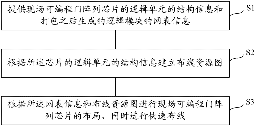
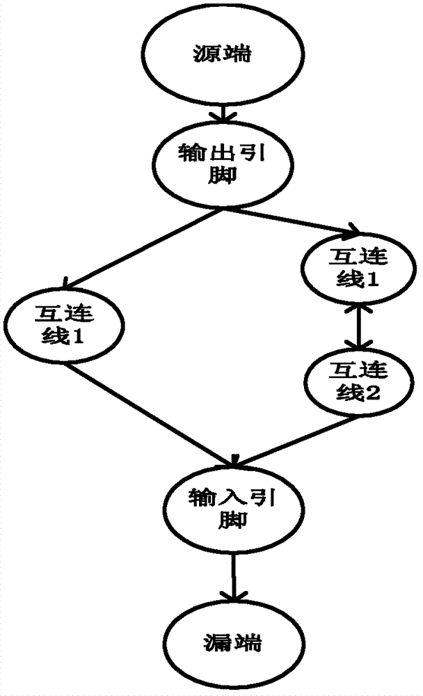
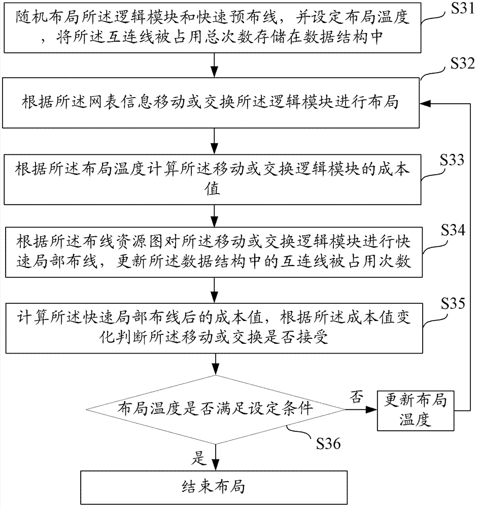
[0040] As mentioned in the background technology, in most of the layout and routing tool software, the relationship between placement an...


PUM


Abstract

The invention provides a field programmable gate array chip layout method. The method includes providing structural information of a logic unit of a field programmable gate array chip and net list information, generated after packaging, of a logic module; establishing a wiring resource map according to the structural information of the logic unit of the chip; arranging the field programmable gate array chip according to the net list information and the wiring resource map, and quickly wiring simultaneously. By the method, quick wiring is realized in the overall arrangement process according to the wiring resource map, and overall arrangement and wiring are closely combined, so that wiring success rate is increased, time delay of a circuit is reduced, and wiring resource utilization rate is increased.

Description

technical field [0001] The invention relates to the fields of integrated circuit design and electronic design automation, in particular to a field programmable gate array chip layout method. Background technique [0002] FPGA (Field-Programmable Gate Array, Field Programmable Gate Array) chip is a programmable device widely used in the market at present, and has the advantages of short development period and low cost. Through the layout of logic modules and the wiring of interconnection lines between logic modules, FPGA chips can realize various applications. Therefore, in the software flow of FPGA design, layout and wiring are crucial steps. The layout determines the position of each logic module required to realize the circuit function in the FPGA chip, and the logic modules are connected by the wiring of the interconnection line. The optimization goal of the layout is to place the connected logic modules close to minimize the required At the same time, it is also necessa...

Claims


Application Information

Patent Timeline
Patent Type & Authority Applications(China)
IPC IPC(8): G06F17/50
Inventor 李明李艳于芳
Owner SOI MICRO CO LTD
Why Eureka
Try Eureka