Semiconductor package structure and manufacturing method thereof

A technology of packaging structure and manufacturing method, which is applied in the direction of semiconductor/solid-state device manufacturing, semiconductor device, semiconductor/solid-state device components, etc. The effect of electrical circuit distance, reduced spacing, and reduced thickness

Active Publication Date: 2016-08-10
CHIPMOS TECH INC
View PDF6 Cites 0 Cited by
  • Summary
  • Abstract
  • Description
  • Claims
  • Application Information

AI Technical Summary

Problems solved by technology

Since the lead frame is currently used to carry the chip, the lead frame still has a certain thickness, and there is a limit to the demand for reducing the pitch, so that the volume and thickness of the overall quad flat no lead package structure cannot be effectively reduced, and Also unable to meet the demand for high bulk density
Furthermore, using bonding wires to electrically connect the chip and the lead frame, the transmission path of the electrical signal is long, which is not conducive to improving the electrical performance, and cannot effectively reduce the volume and thickness of the overall QFN package structure.

Method used


Image

  • Semiconductor package structure and manufacturing method thereof
  • Semiconductor package structure and manufacturing method thereof
  • Semiconductor package structure and manufacturing method thereof

Examples


Embodiment Construction

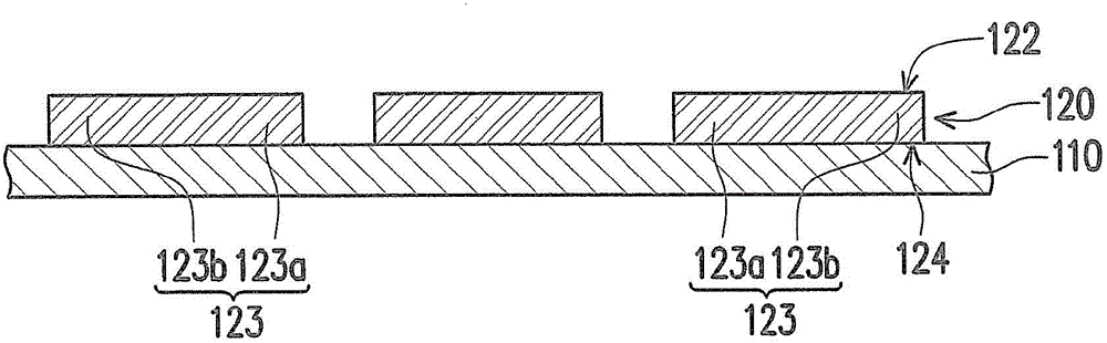
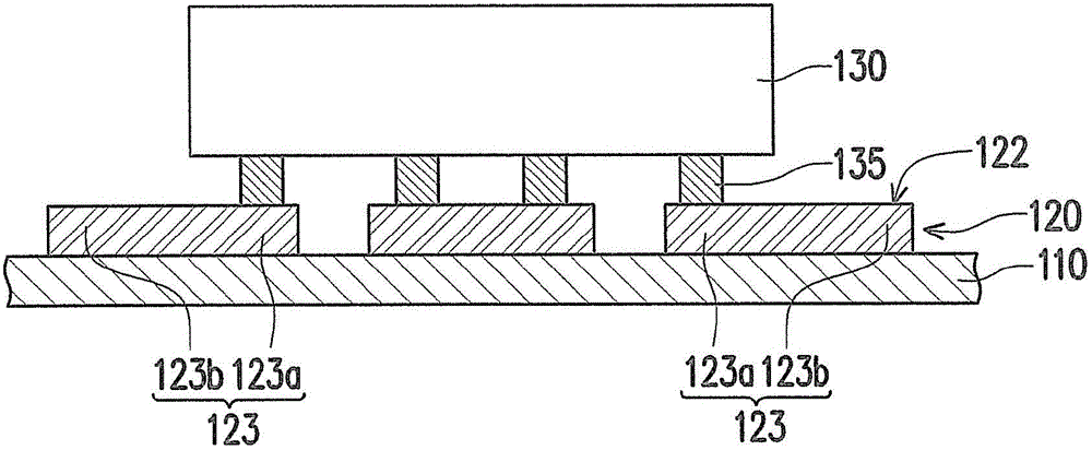
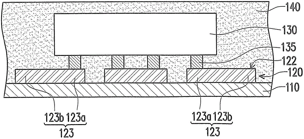
[0046] Figure 1A to Figure 1G It is a schematic cross-sectional view of a manufacturing method of a semiconductor package structure according to an embodiment of the present invention. Please refer to Figure 1A , The manufacturing method of the semiconductor package structure of this embodiment includes the following steps. First, a metal carrier board 110 is provided, and a patterned circuit layer 120 is formed on the metal carrier board 110 . In detail, the patterned circuit layer 120 has an upper surface 122 and a lower surface 124 opposite to each other, wherein the lower surface 124 of the patterned circuit layer 120 faces the metal carrier 110 and is connected to the metal carrier 110 . The patterned circuit layer 120 includes a plurality of circuits 123, and each circuit 123 has a first end 123a and a second end 123b extending from the first end 123a, wherein the second end 123b is away from the first end The direction of the portion 123a extends. In particular, in...


PUM


Abstract

Provided are a semiconductor package structure and a manufacture method thereof. The manufacture method of the semiconductor package structure comprises: forming a patterned circuit layer on a metallic bearing board, wherein the material of the metallic bearing board is different from that of the patterned circuit layer; bonding at least one chip on the metallic bearing board in a flip manner, wherein the chip is electrically connected with the patterned circuit layer; forming packaging colloid on the metallic bearing board so as to cover the chip, the patterned circuit layer, and a part of the metallic bearing board; executing an etching step so as to remove the metallic bearing board until a bottom surface of the patterned circuit layer and a bottom surface of the packaging colloid are exposed; forming an insulating layer on the bottom surface of the patterned circuit layer and the bottom surface of the packaging colloid, wherein the insulating layer comprises multiple openings which expose at least parts of the patterned circuit layer; forming multiple external connection terminals so as to be electrically connected with the exposed patterned circuit layer of the insulating layer.

Description

technical field [0001] The present invention relates to a semiconductor element and its manufacturing method, and in particular to a semiconductor packaging structure and its manufacturing method. Background technique [0002] Semiconductor packaging technology includes many packaging forms, among which the quadrilateral flat no-lead package belonging to the quadrilateral flat package series has a short signal transmission path and relatively fast signal transmission speed, so the quadrilateral flat no-lead package is suitable for high-frequency transmission (such as radio frequency band) chip packaging, and is one of the mainstream low pincount (low pincount) packaging types. [0003] In the manufacturing method of the quad flat no-lead package structure, firstly, a plurality of chips are arranged on a leadframe. Then, the chips are electrically connected to the lead frame by a plurality of bonding wires. Afterwards, a portion of the lead frame, the bonding wires and the ...

Claims


Application Information

Patent Timeline
Patent Type & Authority Patents(China)
IPC IPC(8): H01L21/60H01L21/56H01L23/31
CPCH01L2224/16225H01L2224/48091H01L2224/73265
Inventor 潘玉堂周世文
Owner CHIPMOS TECH INC
Why Eureka
Try Eureka