Method for manufacturing carbon nano tube flexible micro-bumps through transfer method

A carbon nanotube and carbon nanotube bundle technology, which is applied in the field of carbon nanotube flexible bump preparation, can solve the problems of low carbon nanotube bundle array density and the like, achieves good electrical transmission performance, solves electromigration problems, and has the effects of simple process

Active Publication Date: 2013-10-23
NAT CENT FOR ADVANCED PACKAGING
View PDF4 Cites 7 Cited by
  • Summary
  • Abstract
  • Description
  • Claims
  • Application Information

AI Technical Summary

Problems solved by technology

[0007] The production method of the present invention can solve the following problems: one is the problem of producing carbon nanotubes in a high-temperature environment (>600°C), so that carbon nanotubes can be used as interconnect materials on active substrates; The problem of the low density of carbon ...

Method used


Image

  • Method for manufacturing carbon nano tube flexible micro-bumps through transfer method
  • Method for manufacturing carbon nano tube flexible micro-bumps through transfer method
  • Method for manufacturing carbon nano tube flexible micro-bumps through transfer method

Examples


Embodiment Construction

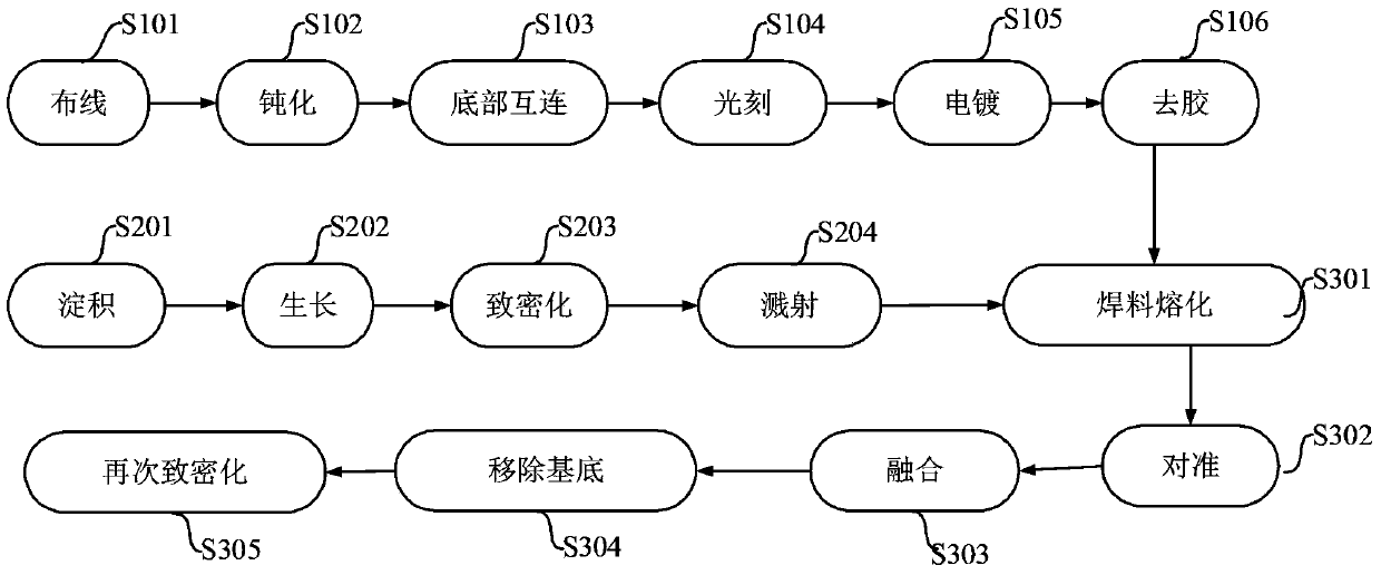
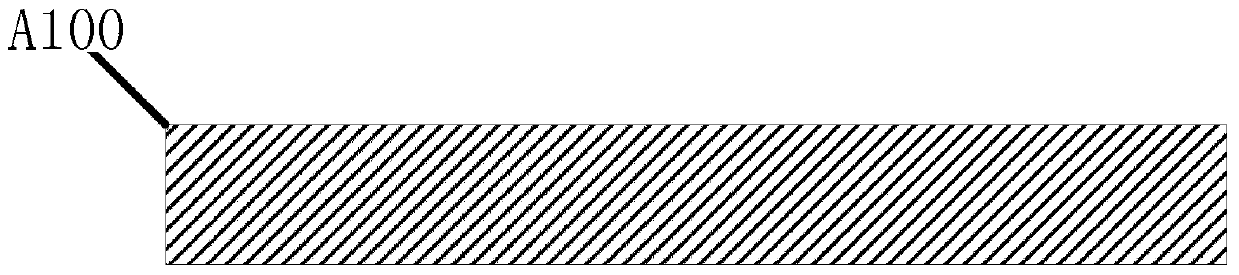
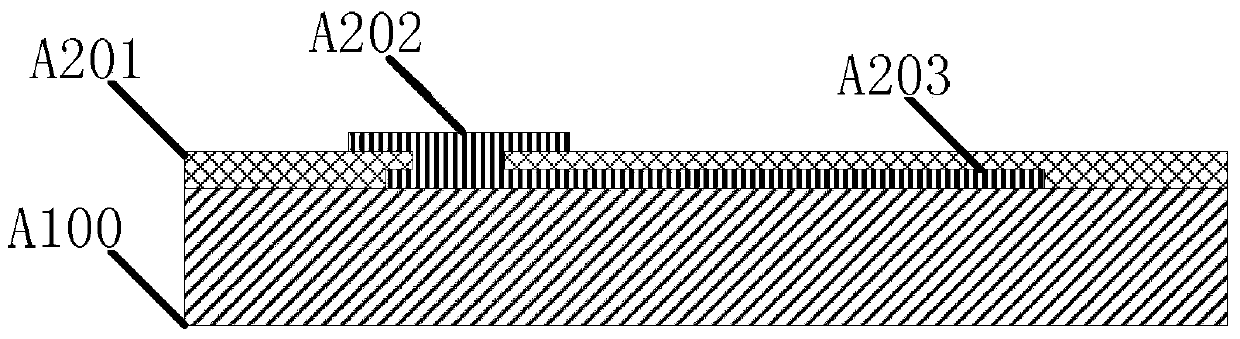
[0062] Embodiments of the present invention are described in detail below.

[0063] Examples of the described embodiments are shown in the drawings, wherein like or similar reference numerals designate like or similar elements or elements having the same or similar functions throughout. The embodiments described below by referring to the figures are exemplary only for explaining the present invention and should not be construed as limiting the present invention. The following disclosure provides many different embodiments or examples for implementing different structures of the present invention. To simplify the disclosure of the present invention, components and arrangements of specific examples are described below. Of course, they are only examples and are not intended to limit the invention. Furthermore, the present invention may repeat reference numerals and / or letters in different instances. This repetition is for the purpose of simplicity and clarity and does not in i...


PUM


Abstract

The invention discloses a method for manufacturing carbon nano tube flexible micro-bumps in microelectronic packaging. According to the method for manufacturing the carbon nano tube flexible micro-bumps, carbon nano tube bundles growing on other substrates are compacted and are transplanted to a semiconductor substrate in a low-temperature transfer manner to obtain flexible micro-bumps. The carbon nano tube bundles have certain elasticity and flexibility, so that the problem of failure caused by thermal stress in interconnection can be solved to a certain extent by manufacturing the flexible micro-bumps through the carbon nano tube bundles. Meanwhile, a carbon nano tube is excellent in electrical performance such as ultrahigh electrical conductivity and current density of over 10<9>A/cm<2>. Therefore, by using the carbon nano tube as micro-bumps, good electrical transmission performance is realized, and the problem of electrical migration of metal bumps can be solved. The method is easy to operate and compatible with a semiconductor process.

Description

technical field [0001] The invention relates to microelectronic packaging technology and micro bump technology, in particular, the invention relates to a method for preparing flexible bumps of carbon nanotubes. Background technique [0002] Flip-chip welding technology is a hybrid integration technology that can facilitate the electrical and mechanical connections between chips. This technology first makes interconnection lead bumps on two chips that need to be interconnected, and then aligns, fuses or bonds these bumps in a dedicated flip-chip bonding device to form an interconnection. Flip-chip packaging technology has the advantages of high precision, small footprint of the formed hybrid integrated chip, high input and output density, short interconnection, and small lead parasitic parameters, which greatly improves the electrical performance and high-frequency performance of the packaged device. In recent years, bump technology in flip-chip soldering has developed rapid...

Claims


Application Information

Patent Timeline
IPC IPC(8): H01L21/60H01L21/768
CPCH01L2224/11
Inventor 戴风伟曹立强周静
Owner NAT CENT FOR ADVANCED PACKAGING
Why Eureka
Try Eureka