Manufacturing method for structure of extremely thin silicon on insulator and manufacturing method for semiconductor device

A technology of silicon-on-insulator and its manufacturing method, which is applied in semiconductor/solid-state device manufacturing, electrical components, circuits, etc., and can solve problems such as uneven and uncontrollable thickness of the top silicon layer 20, affecting the performance of semiconductor devices, etc., so as to save epitaxial growth The effect of the steps

Active Publication Date: 2013-10-23
SEMICON MFG INT (SHANGHAI) CORP
View PDF3 Cites 6 Cited by
  • Summary
  • Abstract
  • Description
  • Claims
  • Application Information

AI Technical Summary

Problems solved by technology

Due to the uneven and uncontrollable thickness of the top silicon layer 20 of the ETSOI structure in the prior art, the performance of the semiconductor device is affected
[0018] Even if the top silicon layer 20 in the semiconductor device is uniform and controllable, the etching process when forming the spacer 25 is likely to etch away all or part of the top silicon layer 20, so that the insulating layer 21 (that is, silicon oxide) cannot be formed. Silicon is epitaxially grown to form raised source 26 and raised drain 27

Method used


Image

  • Manufacturing method for structure of extremely thin silicon on insulator and manufacturing method for semiconductor device
  • Manufacturing method for structure of extremely thin silicon on insulator and manufacturing method for semiconductor device
  • Manufacturing method for structure of extremely thin silicon on insulator and manufacturing method for semiconductor device

Examples


Embodiment Construction

[0072] In order to make the above objects, features and advantages of the present invention more comprehensible, specific implementations of the present invention will be described in detail below in conjunction with the accompanying drawings.

[0073] In the following description, many specific details are set forth in order to fully understand the present invention, but the present invention can also be implemented in other ways than those described here, so the present invention is not limited by the specific embodiments disclosed below.

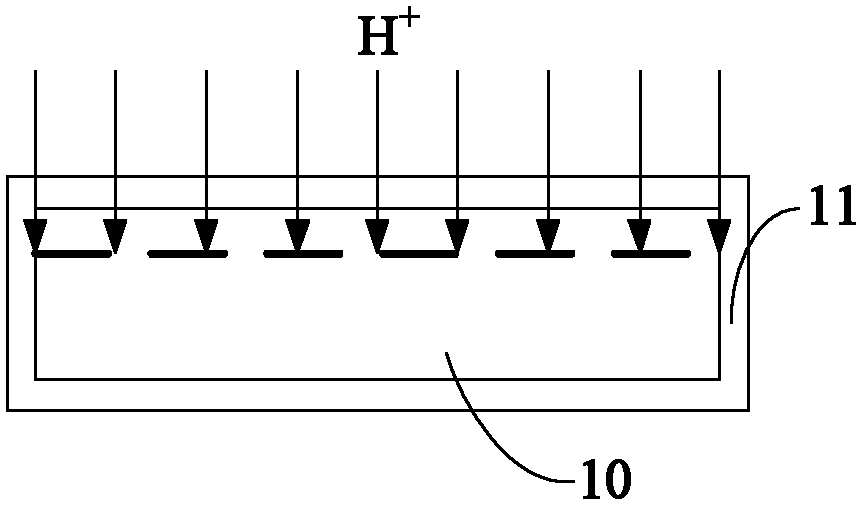
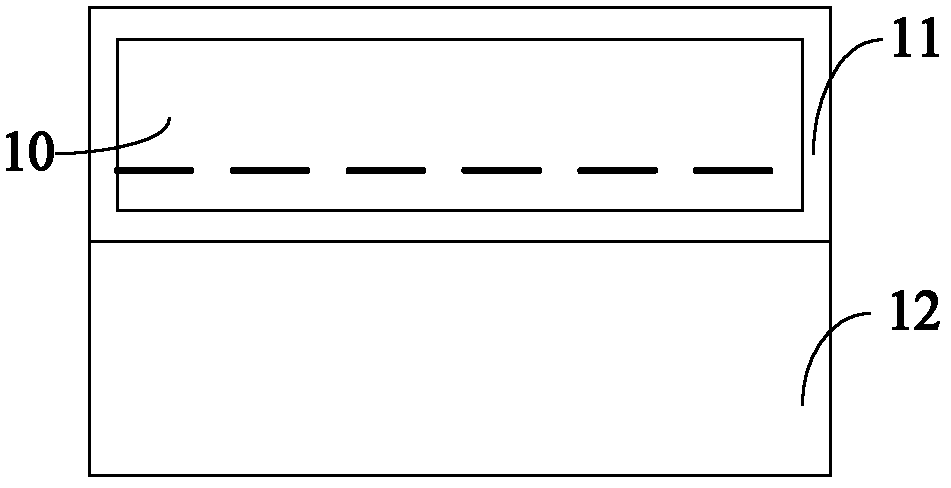
[0074] As mentioned in the background technology section, in the process of making ETSOI in the prior art, the thickness of the top layer of silicon is not easy to be accurately controlled, and its thickness is not uniform; when making semiconductor devices including ETSOI structures, it is easy to damage the top layer of silicon and affect the semiconductor. device performance.

[0075] In view of the above defects, the present invention...


PUM

PropertyMeasurementUnit
thicknessaaaaaaaaaa
thicknessaaaaaaaaaa
thicknessaaaaaaaaaa

Abstract

Disclosed are a manufacturing method for a structure of extremely thin silicon on an insulator (ETSOI) and a manufacturing method for a semiconductor device. The manufacturing method for the semiconductor device includes: providing silicon on insulator (SOI); forming a hard-mask layer on a top-silicon layer and carrying out a patterning processing on the hard-mask layer; and measuring real thicknesses of exposed areas of the top-silicon layer; injecting doping ions into the exposed areas of the top-silicon layer with an injection quantity related to corresponding real thicknesses of the injected areas; carrying out an etching processing, and removing part of the exposed areas of the top-silicon layer and forming trenches; forming side walls on flanks of the trenches and forming gate structures on areas defined by the flanks; carrying out a planarization processing so that upper surfaces of the gate structures are flush with an upper surface of the hard-mask layer; removing the hard-mask layer; and injecting ions into the exposed areas of the top-silicon layer and forming elevated source/drain areas. The manufacturing method for the structure of the extremely thin SOI and the manufacturing method for the semiconductor device enable the thicknesses and uniformity of the areas of the top-silicon layer on the extremely thin SOI structure to be controlled precisely so that damages on the top-silicon layer are prevented.

Description

technical field [0001] The invention relates to the technical field of semiconductors, in particular to a method for manufacturing an ultra-thin silicon-on-insulator structure and a method for manufacturing a semiconductor device including the ultra-thin silicon-on-insulator structure. Background technique [0002] With the development of semiconductor technology, the integration level of integrated circuits is getting higher and higher, and the feature size (CD) of devices is getting smaller and smaller. When the feature size of the device is reduced to deep submicron (under 0.25 micron is called deep submicron), the leakage current of the device increases, the drain induction barrier lower (DIBL, Drain induction barrier lower) effect and the short channel effect (SCE) etc. are becoming more and more obvious, and become the main problem to be overcome in reducing the size of the device. [0003] Semiconductor devices with FDSOI (Fully Depleted Silicon On Insulator, fully d...

Claims


Application Information

Patent Timeline
Patent Type & Authority Applications(China)
IPC IPC(8): H01L21/762
Inventor 陈勇
Owner SEMICON MFG INT (SHANGHAI) CORP
Why Eureka
Try Eureka