Surface plasmon coupling terahertz quantum well detector

A technology of surface plasmons and quantum wells, which is applied in photometry, electrical components, and semiconductor devices using electric radiation detectors, can solve the problems of low responsivity and operating temperature, improve absorption efficiency, and improve device Effect of Responsivity and Operating Temperature

Inactive Publication Date: 2013-10-23
SHANGHAI INST OF MICROSYSTEM & INFORMATION TECH CHINESE ACAD OF SCI
View PDF4 Cites 7 Cited by
  • Summary
  • Abstract
  • Description
  • Claims
  • Application Information

AI Technical Summary

Problems solved by technology

[0005] In view of the above-mentioned shortcomings of the prior art, the object of the present invention is to provide a surface plasmon coupled terahertz quantum well detector, which is used to solve the problem of neutron band absorption efficiency, responsivity and operating temperature in the prior art. low problem

Method used


Image

  • Surface plasmon coupling terahertz quantum well detector
  • Surface plasmon coupling terahertz quantum well detector
  • Surface plasmon coupling terahertz quantum well detector

Examples


Embodiment 1

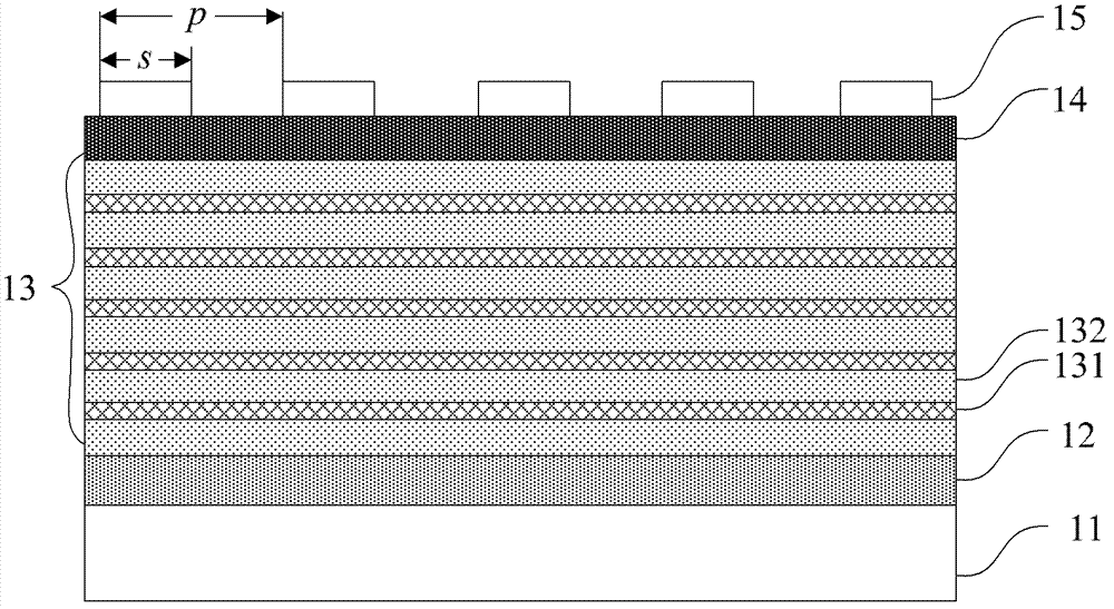
[0031] Such as Figure 1a~1b As shown, the present invention provides a surface plasmon coupled terahertz quantum well detector for detection of incident photons, at least including: a semiconductor substrate 11; a lower electrode 12, combined with the semiconductor substrate 11; The quantum well structure 13, combined with the lower electrode 12, includes a plurality of stacked GaAs / (Al, Ga)As quantum wells, and the GaAs / (Al, Ga)As quantum wells are composed of GaAs layers 131 and (Al, Ga) ) As layer 132; the upper electrode 14 is combined with the multi-quantum well structure 13, and the upper electrode 14 has an electron doping concentration of 1.0×10 17 ~5.0×10 17 / cm 3 The n-type doped n-GaAs layer has a thickness of 0.2-0.6 μm; the metal grating 15, combined with the upper electrode 14, includes a plurality of metal strips arranged at intervals, and the period of the metal grating 15 is 10- 30 μm, the width of the metal strip is 5-15 μm, which is used to realize the p...

Embodiment 2

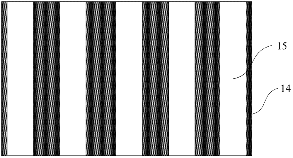
[0034] Such as Figure 1a-3 As shown, this embodiment provides a surface plasmon coupled terahertz quantum well detector for detection of incident photons, at least including: a semiconductor substrate 11; a lower electrode 12, combined with the semiconductor substrate 11; The multi-quantum well structure 13 is combined with the lower electrode 12, including a plurality of stacked GaAs / (Al, Ga)As quantum wells; the upper electrode 14 is combined with the multi-quantum well structure 13, and the upper electrode 14 is The electron doping concentration n is 5.0×10¹⁷ / cm 3 n-type doped n-GaAs layer, the thickness a of which is 0.4 μm; the metal grating 15, combined with the upper electrode 14, includes a plurality of metal strips arranged at intervals, and the period p of the metal grating 15 is 16 μm, The width s of the metal strip is 8 μm, which is used to realize the polar deflection of the incident photons, and make the incident photons interact with the electrons in the uppe...


PUM


Abstract

The invention provides a surface plasmon coupling terahertz quantum well detector, which comprises a semiconductor substrate, a lower electrode, a multi-quantum well structure, an upper electrode and a metal grating, wherein the metal grating is used for realizing polarity deflection of incident photons. The incident photons can be enabled to be interacted with electrons in the upper electrode through adjusting the period of the metal grating, the width of a metal strip, and the electron doping density and the thickness of the upper electrode so as to from surface plasmons on the surface of the upper electrode. The device is located in a sub-wavelength range at a terahertz frequency band because the thickness is only 2-5mum. Therefore, evanescent waves corresponding to the surface plasmons can improve the sub-band absorption efficiency of the device at the resonant frequency, and improves the response rate and the working temperature of the device.

Description

technical field [0001] The invention belongs to the field of semiconductors, in particular to a surface plasmon coupled terahertz quantum well detector. Background technique [0002] Quantum well detector is an important detector working in the mid-to-far infrared and terahertz frequency bands. Terahertz quantum well detector is a photon-type detector with important application prospects in the terahertz frequency band, which has the characteristics of high sensitivity, fast detection speed and narrow-band response. The main structure of this detector includes upper contact layer, multi-quantum well layer and lower contact layer. The number of quantum wells is between 10 and 100, and the thickness of the device is between 2.0 and 5.0 μm in the growth direction of the quantum wells. The bound electrons are introduced into the quantum well by doping. Due to the parabolic energy dispersion relationship, these bound electrons can only absorb photons with an electric field comp...

Claims


Application Information

Patent Timeline
Patent Type & Authority Applications(China)
IPC IPC(8): H01L31/101H01L31/0272H01L31/0304G01J1/42
Inventor 郭旭光曹俊诚张戎张真真谭智勇
Owner SHANGHAI INST OF MICROSYSTEM & INFORMATION TECH CHINESE ACAD OF SCI
Why Eureka
Try Eureka