Light emitting diode with electronic barrier layer structure

An electron blocking layer, light emitting diode technology, applied in circuits, electrical components, semiconductor devices, etc., can solve the problems of LED electron leakage, large lattice mismatch, low compound luminous efficiency, etc., to achieve high energy band gap value, high energy band Offset rate, effect of improving luminous efficiency and ESD yield

Inactive Publication Date: 2013-10-23
SOUTHEAST UNIV
View PDF5 Cites 22 Cited by
  • Summary
  • Abstract
  • Description
  • Claims
  • Application Information

AI Technical Summary

Problems solved by technology

[0007] Purpose of the invention: In order to overcome the deficiencies in the prior art, the present invention provides a light-emitting diode with a new electron blocking layer structure, which can not only solve the problem of electron leakage in the exis...

Method used


Image

  • Light emitting diode with electronic barrier layer structure
  • Light emitting diode with electronic barrier layer structure
  • Light emitting diode with electronic barrier layer structure

Examples


Embodiment Construction

[0019] The present invention will be further described below in conjunction with the accompanying drawings.

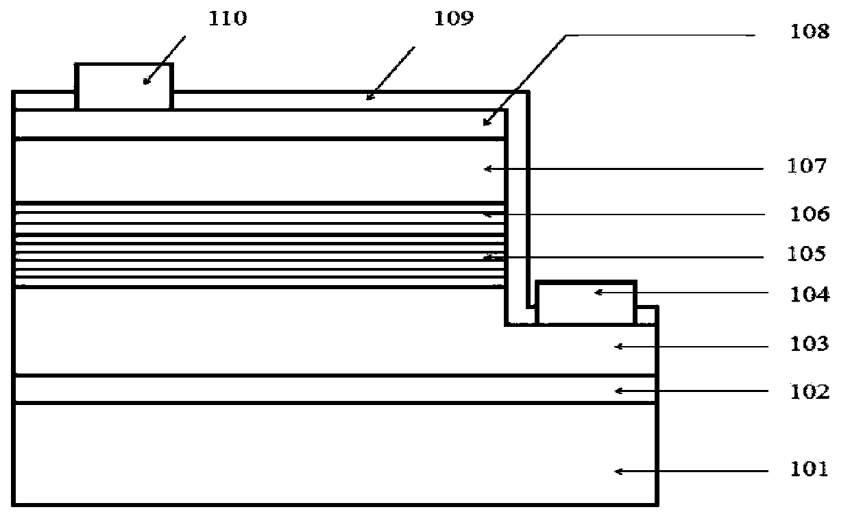
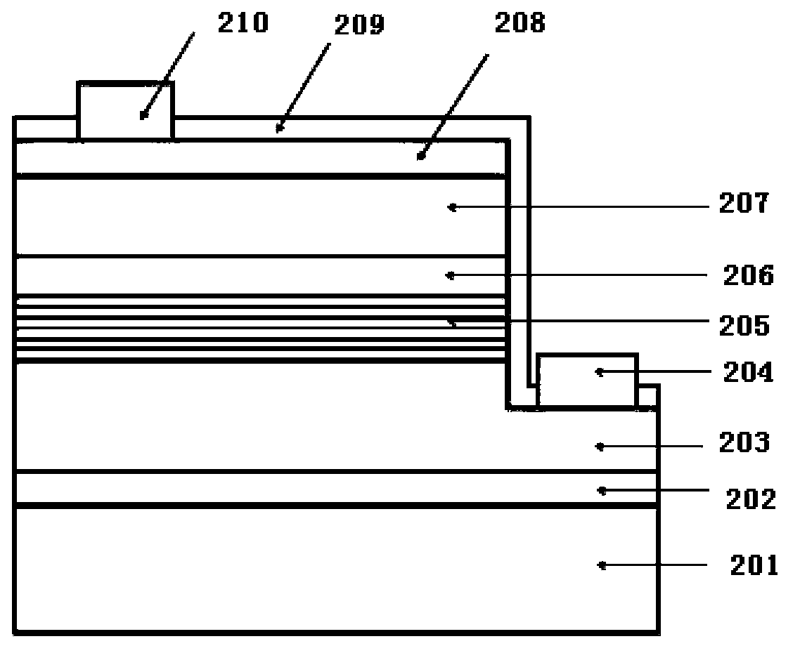
[0020] Such as figure 1Shown: a light-emitting diode with an electron blocking layer structure, including a substrate 101, a buffer layer 102, an n-type GaN epitaxial layer 103, an active light-emitting layer 105 of InGaN / GaN multiple quantum wells, and a p -InAlGaN / GaN electron blocking layer, p-type GaN epitaxial layer 107 and transparent conductive layer 108, the top surface of the transparent conductive layer 108 is provided with a p-type electrode 110, and the n-type GaN epitaxial layer 103 is etched into a ladder shape Mesa, the extension of the step mesa is connected to the bottom surface of the active light-emitting layer 105 of the InGaN / GaN multiple quantum well, the n-type electrode 104 is arranged on the step mesa, and the top surface of the transparent conductive layer 108 is also covered with The passivation layer 109 , the passivation layer 109 extends ...


PUM

PropertyMeasurementUnit
Thicknessaaaaaaaaaa

Abstract

The invention discloses a light emitting diode with an electronic barrier layer structure. The forbidden band width and lattice constant of a quaternary nitride InxAlyGa1-x-yN can be independently adjusted, the In and Al ingredients in p-InxAlyGa1-x-yN are adjusted to match with the lattice between GaN in a binary nitride or a ternary nitride or a InGaN/GaN multi-quantum well and the GaN in a p type GaN epitaxial layer so as to obtain high energy band gap value and energy band offset ratio, effectively reduce the electron leakage rate and improve the injection efficiency of holes, thereby greatly improving the light emission efficiency and ESD yield of LED devices.

Description

technical field [0001] The invention belongs to the technical field of semiconductor lighting, and in particular relates to a light emitting diode with an electron blocking layer structure. Background technique [0002] LED is currently the most widely used device in the field of semiconductor lighting. Its advantages of high efficiency, energy saving, environmental protection, long life and low power consumption make it have a very good application prospect in the field of dynamic display and industrial lighting. [0003] With the continuous improvement of epitaxial growth technology, the optoelectronic performance of GaN-based LEDs has been significantly improved. In order to realize high-performance LED devices, it is necessary to further improve the ESD yield and luminous efficiency of LEDs. Researchers have experimented (Yun Yan Zhang and Yi An Yin, "Performance enhancement of blue light-emitting diodes with a special designed AlGaN / GaN superlattice electron-blocking l...

Claims


Application Information

Patent Timeline
IPC IPC(8): H01L33/14H01L33/06
Inventor 张雄朱敏崔一平
Owner SOUTHEAST UNIV
Why Eureka
Try Eureka