Method for subjecting red light semiconductor laser device to Zn diffusion operation

A laser and semiconductor technology, used in semiconductor lasers, lasers, laser parts, etc., can solve the problems of inability to precisely control process parameters and inability to achieve mass production.

Active Publication Date: 2013-10-23
Shandong Huaguang Optoelectronics Co. Ltd.
View PDF6 Cites 6 Cited by
  • Summary
  • Abstract
  • Description
  • Claims
  • Application Information

AI Technical Summary

Problems solved by technology

[0007] Aiming at the problem that the process parameters in the prior art of red semiconductor laser adopting a closed tube method for Zn diffusion cannot be precisely controlled and mass production cannot be realized, the present invention provides a

Method used


Image

  • Method for subjecting red light semiconductor laser device to Zn diffusion operation
  • Method for subjecting red light semiconductor laser device to Zn diffusion operation
  • Method for subjecting red light semiconductor laser device to Zn diffusion operation

Examples


Embodiment 1

[0050] Utilize MOCVD to carry out the method for Zn diffusion of red light semiconductor laser, the steps are as follows:

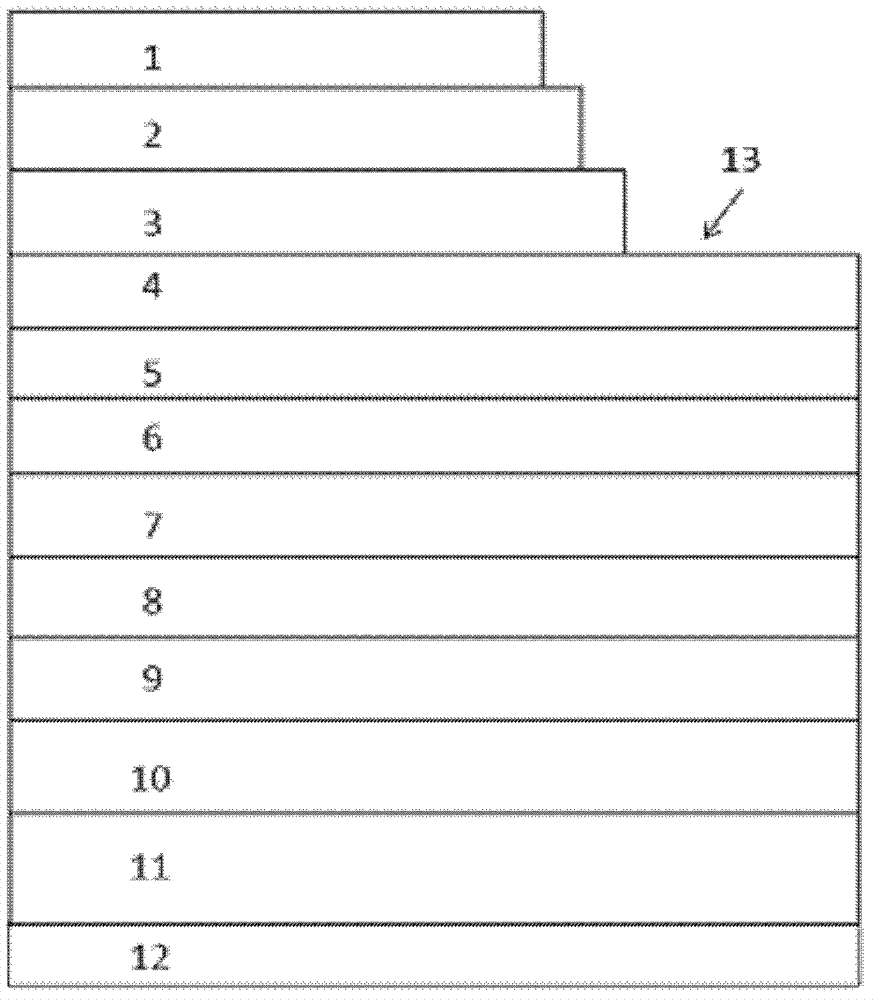
[0051] Step 1. Deposit an epitaxial layer on the semiconductor substrate by MOCVD, and the epitaxial layer includes: a buffer layer, an n-type confinement layer, an N-region intrinsic waveguide layer, an intrinsic compressive strain multi-quantum well active region, and a P-region intrinsic waveguide layer. Sign waveguide layer, p-type confinement layer, GaInP and ohmic contact layer.

[0052] The buffer layer 10 is made of Si-doped GaAs material, and the concentration of doped atoms is 1E18 atoms / cm 3 , with a thickness of 0.5 microns; the n-type confinement layer 9 is made of Al 0.5 In 0.5 P(AlInP) material, the concentration of doped atoms is 1E18 atoms / cm 3 , with a thickness of 11 microns; the N-region intrinsic waveguide layer 8 adopts (AlxGal-x) 0.5 In 0.5 P(AlGaInP) material with a thickness of 0.2 microns; the intrinsic compressive strain mu...

Embodiment 2

[0060] Embodiment 2: The difference from Embodiment 1 is the difference in the structure of the epitaxial layer of the laser and the change of the process conditions for Zn expansion

[0061] Another epitaxial structure adopted is mainly to add a GaInP layer between the buffer layer and the n-type confinement layer to ensure the stability of the lattice transition, and the thickness of each layer is also different.

[0062] Step 1, using MOCVD to deposit an epitaxial layer on the semiconductor substrate, the epitaxial layer includes: buffer layer, GaInP, n-type confinement layer, intrinsic waveguide layer, intrinsic compressive strain multi-quantum well active region, p-type confinement layer, GaInP and ohmic contact layer.

[0063] The buffer layer 10 is made of silicon-doped GaAs material, and the concentration of doped atoms is 1E18 atoms / cm 3 , with a thickness of 0.5 microns; the GaInP layer 4 has a thickness of 0.02 microns; the n-type confinement layer 9 adopts (AlxGal...


PUM


Abstract

The invention provides a method for subjecting a red light semiconductor laser device Zn diffusion operation. The method comprises the following steps: An MOCVD device is used, the laser device is put in a reaction chamber, AsH3 is introduced into the reaction chamber when temperature in the reaction chamber rises to 200 DEG C to 350 DEG C, dimethyl zinc is introduced into the reaction chamber for cavity surface diffusion when the temperature rises to 400 DEG C, the temperature is kept constant for 20 min to 70 min when rising to 450 DEG C to 650 DEG C, annealing operation is performed when the temperature falls to 150 DEG C to 300 DEG C within 15 min to 30 min, and Zn diffusion is finished when the temperature in the reaction chamber falls below 100 DEG C. The method of the invention is advantageous in that uniform Zn diffusion, ease of control and large production capacity are realized; Zn diffusion of tens of laser devices can be finished in one time; the output power of the laser device adopting a Zn diffusion mode for making a non-absorption window is 10% higher than the power of a laser device adopting a closed-tube Zn diffusion mode.

Description

technical field [0001] The invention relates to a Zn diffusion method for a red light semiconductor laser by metal organic compound vapor deposition (MOCVD), which belongs to the technical field of semiconductors. Background technique [0002] AlGaInP quaternary material red light semiconductor lasers are small in size, light in weight and low in energy consumption. Such devices are widely used in optical disc recording, information storage, barcode scanning, laser ranging, gas detection and medical equipment and other fields. In order to meet the requirements of the market for laser output power, it has become a technical hotspot in this field to improve the laser output power by optimizing the laser material, device structure and manufacturing process. [0003] The thermal conductivity and conduction band difference of AlGaInP material, and the bandgap difference with lower valence band difference have a greater impact on the output power, differential quantum efficiency a...

Claims


Application Information

Patent Timeline
IPC IPC(8): H01S5/343
Inventor 张新徐现刚张雨吴德华夏伟
Owner Shandong Huaguang Optoelectronics Co. Ltd.
Why Eureka
Try Eureka