Preparation method of silicon oxynitride thin film

A technology of silicon oxynitride and manufacturing method, which is applied in semiconductor/solid-state device manufacturing, electrical components, circuits, etc., can solve the problems of strong reading and writing performance and unstable product performance, achieve stable reading and writing performance, and reduce reading and writing performance. , the effect of uniform oxygen content

Inactive Publication Date: 2013-10-30
SHANGHAI HUAHONG GRACE SEMICON MFG CORP
View PDF4 Cites 3 Cited by
  • Summary
  • Abstract
  • Description
  • Claims
  • Application Information

AI Technical Summary

Problems solved by technology

Finally, when using the silicon oxynitride film formed by the existing process to make the ONO layer and finally make the flash memory product, the read and write performance of the product will be related to the actual position of the product in the device when the silicon oxynitride film of the ONO layer is formed Very strong, making the performance of the product unstable

Method used


Image

  • Preparation method of silicon oxynitride thin film
  • Preparation method of silicon oxynitride thin film
  • Preparation method of silicon oxynitride thin film

Examples


Embodiment Construction

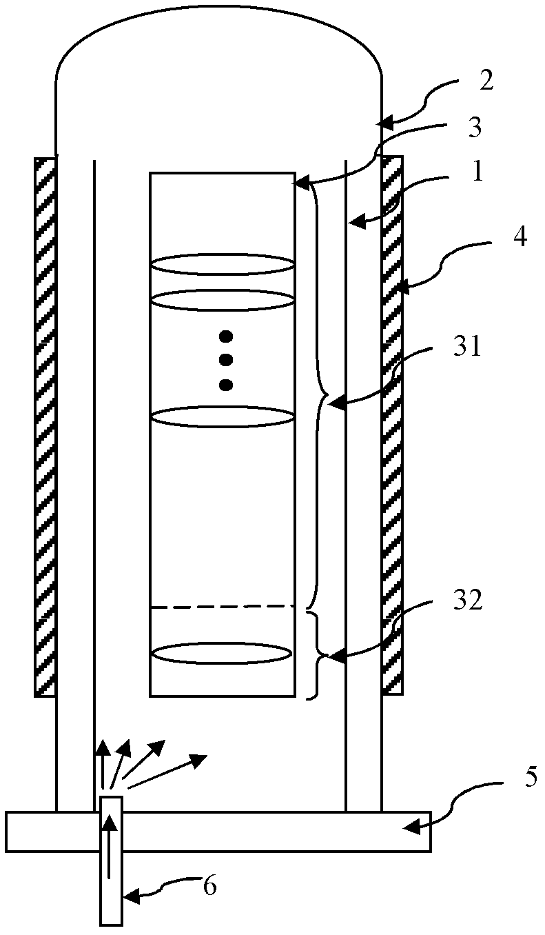
[0022] The manufacturing method of embodiment of the present invention-silicon oxynitride thin film adopts such as figure 1 The shown vertical LP CVD furnace tube grows a silicon oxynitride film, and the silicon wafer product is placed in the product operation area 31 of the vertical LP CVD furnace tube, and in the accompanying sheet placement area of ​​the vertical LP CVD furnace tube 32 Place a quartz sheet, the diameter of the quartz sheet is the same as that of the silicon sheet product and both are 8 inches, and the thickness of the quartz sheet is more than 3 mm.

[0023] When the silicon oxynitride film is grown, the process gases used include: dichlorosilane (DCS), nitrous oxide and ammonia gas, which are silicon source, oxygen source and nitrogen source for forming the silicon oxynitride film respectively. Various process gases are equipped with different inlet pipes 6 respectively, and various process gases enter the bottom of the reaction chamber through their respe...


PUM

PropertyMeasurementUnit
thicknessaaaaaaaaaa

Abstract

The invention discloses a preparation method of a silicon oxynitride thin film. A vertical LPCVD furnace tube is used for performing silicon oxynitride thin film growing. A silicon chip product is placed in a product work area of the vertical LPCVD furnace tube. An oxygen source, which is nitrogen monoxide, of the silicon oxynitride thin film is formed. Before the nitrogen monoxide going into the product work area and participating in reactors to form the silicon oxynitride thin film, the nitrogen monoxide is preheated and then is fully decomposed. According to the preparation method of the silicon oxynitride thin film, a correlation between oxygen content of the silicon oxynitride thin film and actual positions of the product in the furnace tube is substantially reduced, so that oxygen content of the silicon oxynitride thin film in different positions in the furnace tube is uniform, the RI in-furnace uniformity of the silicon oxynitride thin film is improved, and performance of the product is stabilized.

Description

technical field [0001] The invention relates to a manufacturing process method of a semiconductor integrated circuit, in particular to a manufacturing method of a silicon oxynitride film. Background technique [0002] Flash memory (Flash) generally includes a floating gate electrode to store charges. In the prior art, an oxide-nitride-oxide (ONO) structure is generally used as a floating gate electrode. The process for preparing the ONO layer is Flash manufacturing. One of the key processes in the existing ONO layer includes a four-layer structure, the four-layer thin film is respectively, the tunnel oxide layer, the first layer of silicon oxynitride layer (SiON), the second layer of silicon oxynitride layer, barrier Oxide layer: The tunnel oxide layer is generally formed by dry oxygen oxidation or wet oxygen oxidation (TOX) process, and the barrier oxide layer is generally formed by high temperature oxide deposition (HTO) of low pressure chemical vapor deposition (LPCVD) pr...

Claims


Application Information

Patent Timeline
Patent Type & Authority Applications(China)
IPC IPC(8): H01L21/283
Inventor 杨继业姚毅
Owner SHANGHAI HUAHONG GRACE SEMICON MFG CORP
Why Eureka
Try Eureka