a bi 2 the se 3 Silicon Schottky junction with thin film as contact layer and preparation method

A Schottky junction and contact layer technology, which is applied in the direction of electrical components, circuits, semiconductor devices, etc., can solve the problems of unsuitability for large-scale production, deterioration of silicon Schottky junction characteristics, and unguaranteed quality of heterojunction interfaces and other problems, to achieve excellent optical and electrical properties, reduce Si surface state density, and ideal characteristics

Active Publication Date: 2016-08-10
UNIV OF ELECTRONICS SCI & TECH OF CHINA
View PDF2 Cites 0 Cited by
  • Summary
  • Abstract
  • Description
  • Claims
  • Application Information

AI Technical Summary

Problems solved by technology

[0006] The present invention provides a 2 Se 3 The thin film is the silicon Schottky junction of the contact layer and its preparation method, which solves the problem of Bi 2 Se 3 The thin film may cause the deterioration of the characteristics of the silicon Schottky junction. In addition, the traditional Bi 2 Se 3 The single crystal sheet is mechanically pasted on the Si sheet, which is not suitable for large-scale production, and the quality of the heterojunction interface cannot be guaranteed

Method used


Image

  • a bi  <sub>2</sub> the se  <sub>3</sub> Silicon Schottky junction with thin film as contact layer and preparation method
  • a bi  <sub>2</sub> the se  <sub>3</sub> Silicon Schottky junction with thin film as contact layer and preparation method
  • a bi  <sub>2</sub> the se  <sub>3</sub> Silicon Schottky junction with thin film as contact layer and preparation method

Examples


Embodiment 1

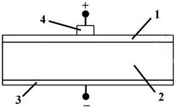
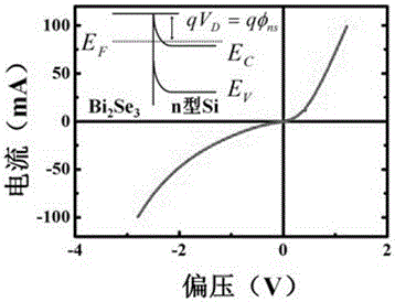
[0030] like figure 1 As shown, the present embodiment includes n-type Si substrate 2, the resistivity of Si substrate 2 is 0.001Ω·cm, and the top of Si substrate 2 is provided with Bi 2 Se 3 Schottky contact layer 1, Bi 2 Se 3 The thickness of Schottky contact layer 1 is 5nm, and the bottom of Si substrate 2 is provided with ohmic contact back electrode 3, Bi 2 Se 3 The Schottky contact layer 1 is provided with an ohmic contact electrode 4 made of Al with a thickness of 20nm, Bi 2 Se 3 An adhesive layer is provided between the Schottky contact layer 1 and the ohmic contact electrode 4, and the adhesive layer is made of Cr.

[0031] Preferably, the Si substrate 2 in this embodiment is a (111)-oriented single crystal.

[0032] A Bi 2 Se 3 A method for preparing a silicon Schottky junction with a thin film as a contact layer, comprising the following steps:

[0033] (a) After the Si substrate with the crystal orientation of (111) is cleaned by RCA chemical cleaning meth...

Embodiment 2

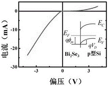
[0040] like figure 1 As shown, the present embodiment includes a p-type Si substrate 2, the resistivity of the Si substrate 2 is 10Ω·cm, and the top of the Si substrate 2 is provided with a thickness of 27.5nm. 2 Se 3 Schottky contact layer 1, the bottom of Si substrate 2 is provided with ohmic contact back electrode 3, Bi 2 Se 3 The Schottky contact layer 1 is provided with an ohmic contact electrode 4 made of Ag and having a thickness of 110 nm, Bi 2 Se 3 An adhesive layer is provided between the Schottky contact layer 1 and the ohmic contact electrode 4, and the adhesive layer is made of Ti.

[0041] Preferably, the Si substrate 2 in this embodiment is a (111)-oriented single crystal.

[0042] A Bi 2 Se 3 A method for preparing a silicon Schottky junction with a thin film as a contact layer, comprising the following steps:

[0043] (a) After the Si substrate with the crystal orientation of (111) is cleaned by RCA chemical cleaning method, the chemical passivation pr...

Embodiment 3

[0050] like figure 1 As shown, the present embodiment includes a type that is close to the high-resistance n-Si substrate 2 of intrinsic conductance, the resistivity of Si substrate 2 is 5000Ω·cm, and the top of Si substrate 2 is provided with the Bi that thickness is 50nm 2 Se 3Schottky contact layer 1, the bottom of Si substrate 2 is provided with ohmic contact back electrode 3, Bi 2 Se 3 The Schottky contact layer 1 is provided with an ohmic contact electrode 4 made of Au with a thickness of 200nm, Bi 2 Se 3 An adhesive layer is provided between the Schottky contact layer 1 and the ohmic contact electrode 4, and the adhesive layer is made of Cr.

[0051] Preferably, the Si substrate 2 in this embodiment is a (111)-oriented single crystal.

[0052] A Bi 2 Se 3 A method for preparing a silicon Schottky junction with a thin film as a contact layer, comprising the following steps:

[0053] (a) After the Si substrate with the crystal orientation of (111) is cleaned by RC...


PUM


Abstract

The invention discloses a silicon Schottky junction with a Bi2Se3 thin film as a contact layer and a preparation method thereof. The silicon Schottky junction includes a Si substrate, and a Bi2Se3 Schottky contact layer is arranged on the upper part of the Si substrate. The bottom of the sheet is provided with an ohmic contact back electrode, the Bi2Se3 Schottky contact layer is provided with an ohmic contact electrode, and an adhesive layer is provided between the Bi2Se3 Schottky contact layer and the ohmic contact electrode, and the adhesive layer is made of Cr Or made of Ti. The present invention adopts the above-mentioned structure, which can form a stable Schottky junction between Bi2Se3 and n-type Si. In addition, the adhesive layer can effectively paste the Bi2Se3 single crystal sheet and the Si sheet together, which is suitable for large-scale production. And the quality of the heterojunction interface can be guaranteed.

Description

technical field [0001] The present invention relates to topological insulator bismuth selenide (Bi 2 Se 3 ) and silicon (Si) material-level integration of spin or photovoltaic device applications, especially a method of preparing single crystal structure Bi on the surface of Si(111)-1×1 after passivation of hydrogen atoms by physical vapor deposition technology 2 Se 3 Method of topological insulator thin film contact layer to form Schottky junction. Background technique [0002] Silicon is known to be the most commercially valuable microelectronic and photovoltaic material. Si-based Schottky diodes are majority-carrier devices with small junction capacitance and fast working speed, and are widely used in high-speed integrated circuits and photovoltaic fields. However, the current conventional metal (metal silicide) / Si Schottky junction devices have been developed very maturely, so finding electrode materials with superior and novel physical properties to expand the appli...

Claims


Application Information

Patent Timeline
Patent Type & Authority Patents(China)
IPC IPC(8): H01L29/47H01L21/28H01L31/0224
Inventor 李含冬高磊李辉王高云罗思源任武洋艾远飞巫江周志华王志明
Owner UNIV OF ELECTRONICS SCI & TECH OF CHINA
Why Eureka
Try Eureka