Miniaturized substrate integration waveguide duplexer

A substrate-integrated waveguide and duplexer technology, which is applied to waveguide-type devices, electrical components, circuits, etc., can solve the problems of high processing cost, large duplexer volume, and difficulty in integration, and achieves fast processing cycle and eliminates area. , easy-to-integrate effects

Active Publication Date: 2013-11-13
JIANGSU HENGXIN TECH CO LTD
View PDF3 Cites 17 Cited by
  • Summary
  • Abstract
  • Description
  • Claims
  • Application Information

AI Technical Summary

Problems solved by technology

[0004] The purpose of the present invention is to propose a miniaturized substrate-integrated waveguide duplexer, which overcomes the shortcomings of existing duplexers such as large volume, high processing cost and difficulty in integration.

Method used


Image

  • Miniaturized substrate integration waveguide duplexer
  • Miniaturized substrate integration waveguide duplexer

Examples


Embodiment Construction

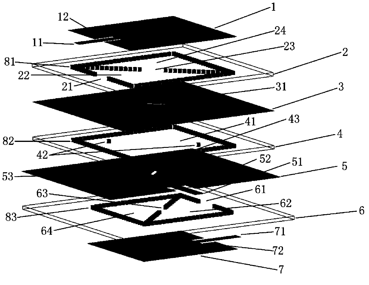
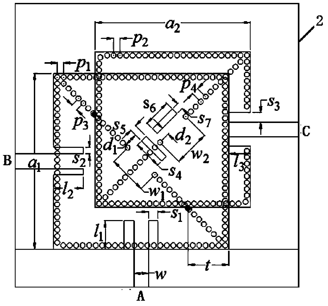
[0013] The present invention will be further described below in conjunction with accompanying drawing and specific embodiment: figure 1 As shown, the miniaturized substrate-integrated waveguide duplexer is characterized in that it includes a first metal copper clad layer 1, a first dielectric layer 2, a second metal copper clad layer 3, and a second dielectric layer stacked sequentially from top to bottom. Layer 4, the third metal copper clad layer 5, the third dielectric layer 6, the fourth metal copper clad layer 7; the metallized through hole array 81 runs through the first metal copper clad layer 1, the first dielectric layer 2, the second metal clad layer The second metal clad copper layer 3 forms a triangular resonant cavity 1 22 and a triangular resonant cavity 2 24 of the same size. These two triangular resonant cavities are isosceles right triangles; Metallized through-holes 42 penetrate the second metal copper-clad layer 3, the second dielectric layer 4, and the thir...


PUM

PropertyMeasurementUnit
thicknessaaaaaaaaaa
isolationaaaaaaaaaa

Abstract

The invention discloses a miniaturized substrate integration waveguide duplexer which comprises a first metal copper coating layer, a first dielectric layer, a second metal copper coating layer, a second dielectric layer, a third metal copper coating layer, a third dielectric layer and a fourth metal copper coating layer which are stacked from the top down sequentially, wherein a dual-mode resonant cavity and triangular resonant cavities are defined by metallized through hole arrays; the dual-mode resonant cavity is connected with the triangular resonant cavities by coupling slots; the triangular resonant cavities are connected mutually by coupling windows; and a microstrip line structure is used for input and output. The duplexer can be used for microwave and millimeter wave communication systems, and has the advantages that the duplexer is suitable for system miniaturization, and is light in weight, low in cost, easy to integrate and fast in processing cycle.

Description

technical field [0001] The invention belongs to the technical field of microwave and millimeter wave passive devices, in particular to a substrate integrated waveguide duplexer in microwave and millimeter wave passive devices. Background technique [0002] With the rapid development of modern communication systems, the functions of microwave and millimeter wave circuits are becoming more and more complex, and the electrical performance requirements are getting higher and higher. At the same time, they are also developing in the direction of miniaturization, light weight, and low cost. This development trend is formed to meet the commercial requirements of microwave and millimeter wave circuits. The substrate integrated waveguide is a kind of transmission line structure with low loss, high power capacity, low cost and easy integration under this situation. Using this technology, high-performance filters, antennas, duplex Microwave and millimeter wave devices such as devices....

Claims


Application Information

Patent Timeline
Patent Type & Authority Applications(China)
IPC IPC(8): H01P1/205H01P11/00
Inventor 林先其程飞张瑾于家伟宋开军樊勇
Owner JIANGSU HENGXIN TECH CO LTD
Why Eureka
Try Eureka