Frame based flat package part manufacturing process adopting cutting channel optimization technology

A technology of flat packaging and manufacturing process, which is applied in semiconductor/solid-state device manufacturing, electrical components, electric solid-state devices, etc., and can solve problems such as defective products, reduced product packaging reliability, and delamination

Inactive Publication Date: 2013-11-20
HUATIAN TECH XIAN
View PDF3 Cites 2 Cited by
  • Summary
  • Abstract
  • Description
  • Claims
  • Application Information

AI Technical Summary

Problems solved by technology

However, most semiconductor packaging manufacturers currently face some process confusion in the QFN/DFN manufacturing process. The reason is that in the plastic packaging process of the existing QFN/DFN process, due to the limitations of the frame structure, the defect prevention of the stepped lead frame used ( layered) process measures are no

Method used


Image

  • Frame based flat package part manufacturing process adopting cutting channel optimization technology
  • Frame based flat package part manufacturing process adopting cutting channel optimization technology
  • Frame based flat package part manufacturing process adopting cutting channel optimization technology

Examples


Embodiment Construction

[0024] The invention will be further described below according to the accompanying drawings.

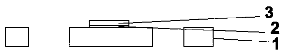
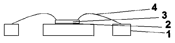
[0025] Such as Figure 8 As shown, a frame-based flat package is mainly composed of a lead frame 1 , a die-bonding glue 2 , a chip 3 , a bonding wire 4 and a plastic package 5 . The lead frame 1 and the chip 3 are connected by the adhesive 2 , the bonding wire 4 connects the lead frame 1 and the chip 3 , and the plastic package 5 surrounds the lead frame 1 , the adhesive 2 , the chip 3 and the bonding wire 4 . The plastic package 5 supports and protects the chip 3 and the bonding wire 4 . The chip 3, the bonding wire 4, the plastic package 5, and the lead frame 1 constitute the power supply and signal channel of the circuit.

[0026] The process flow of a flat package based on frame-based dicing line optimization technology is as follows: wafer thinning→scribing→die (bonding)→bonding→plastic sealing→post-curing→etching dicing lines→cutting→inspection→packaging → Storage.

[0027]...


PUM


Abstract

The invention discloses a frame based flat package part manufacturing process adopting the cutting channel optimization technology. The manufacturing process comprises the steps of wafer thinning, scribing, chip loading (chip bonding), pressure welding, plastic packaging, post curing, cutting channel etching, cutting, detecting, packaging and warehousing. The frame based flat package part manufacturing process can effectively avoid burring and layering of products in the procedure of cutting, thereby further improving the reliability of the products.

Description

[0001] technical field [0002] The invention relates to the technical field of integrated circuit packaging, in particular to a manufacturing process of a flat package based on a frame and adopting a cutting line optimization technology. Background technique [0003] QFN (four-sided flat no-lead package) and DFN (dual flat no-lead package) packages have been developed in recent years with the emergence of communication and portable small digital electronic products (digital cameras, mobile phones, PCs, MP3) , Applicable to the packaging of small and medium-sized integrated circuits with electrical requirements such as high frequency, broadband, low noise, high thermal conductivity, small volume, and high speed. The QFN / DFN package effectively utilizes the package space of the lead pins, thereby greatly improving the package efficiency. However, most semiconductor packaging manufacturers currently face some process confusion in the QFN / DFN manufacturing process. The reason ...

Claims


Application Information

Patent Timeline
IPC IPC(8): H01L21/98
CPCH01L2224/48091H01L2224/48247H01L2224/92247H01L2224/97H01L2924/181H01L2924/00014H01L2924/00012
Inventor 李万霞李站崔梦魏海东
Owner HUATIAN TECH XIAN
Why Eureka
Try Eureka