One-dimensional electronic gas GaN-based HEMT (High Electron Mobility Transistor) device adopting selective area epitaxy and preparation method thereof

A selective area epitaxy, electron gas technology, applied in the field of microelectronics, can solve the problems of small breakdown electric field, limited electron concentration, poor electron transport characteristics, etc., to achieve the effect of improving high temperature and high pressure characteristics, improving power characteristics, and good power characteristics

Active Publication Date: 2013-11-20
云南凝慧电子科技有限公司
View PDF9 Cites 2 Cited by
  • Summary
  • Abstract
  • Description
  • Claims
  • Application Information

AI Technical Summary

Problems solved by technology

[0017] one. Due to the small bandgap of Si and GaAs semiconductor materials, the intrinsic carrier concentration is high and the breakdown electric field is small, which makes the prepared Si-based and GaAs-based devices have poor high-temperature and high-voltage characteristics and poor radiation resistance. weak;
[0018] two. Due to the poor electron transport characteristics

Method used


Image

  • One-dimensional electronic gas GaN-based HEMT (High Electron Mobility Transistor) device adopting selective area epitaxy and preparation method thereof
  • One-dimensional electronic gas GaN-based HEMT (High Electron Mobility Transistor) device adopting selective area epitaxy and preparation method thereof
  • One-dimensional electronic gas GaN-based HEMT (High Electron Mobility Transistor) device adopting selective area epitaxy and preparation method thereof

Examples


Embodiment 1

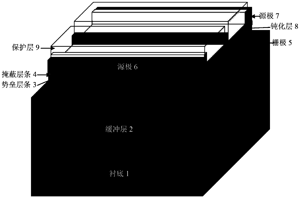
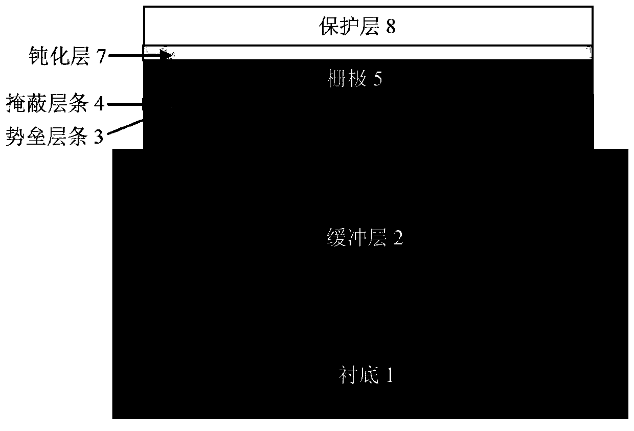
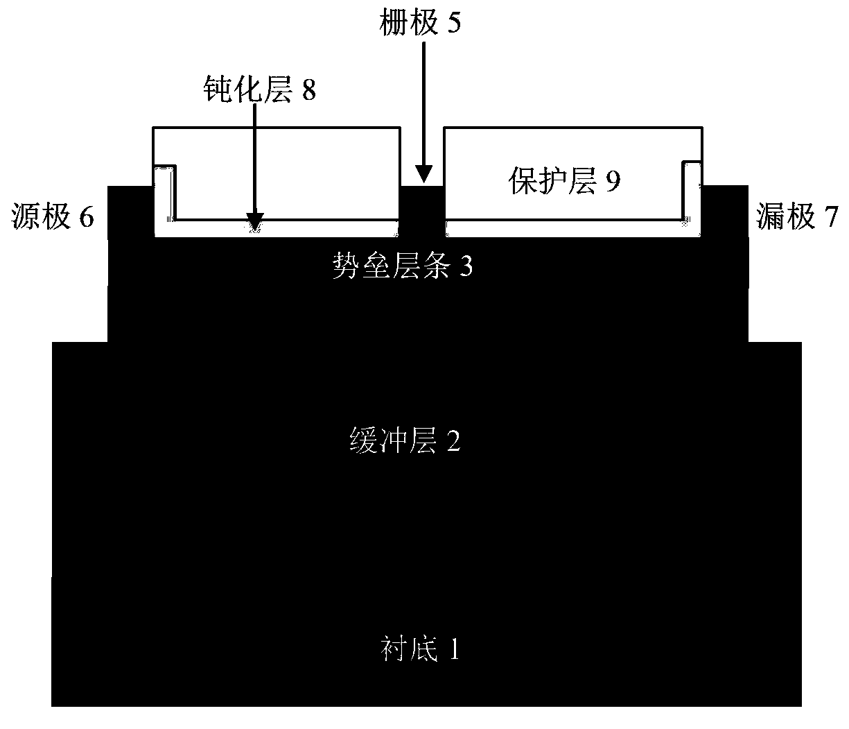
[0073] The device structure of embodiment 1 is: substrate 1 is sapphire, buffer layer 2 is GaN, barrier layer bar 3 is AlGaN, passivation layer 8 is SiN, protective layer 9 is SiN, masking layer bar 4 is SiN, masking layer The strip 4 has a thickness of 10nm and a width of 50nm, the barrier layer strip 3 has a width of 10nm, and the masking layer strip 4 and the barrier layer strip 3 are arranged periodically at intervals;

Embodiment 2

[0074] The device structure of Example 2 is: the substrate 1 is silicon carbide, the buffer layer 2 is GaN, the barrier layer strip 3 is AlGaN, the passivation layer 8 is SiN, and the protective layer 9 is SiO 2 , the masking layer strip 4 is SiN, the thickness of the masking layer strip 4 is 30nm, the width is 250nm, the width of the barrier layer strip 3 is 50nm, and the masking layer strip 4 and the barrier layer strip 3 are periodically arranged at intervals;

Embodiment 3

[0075] The device structure of Example 3 is: the substrate 1 is silicon, the buffer layer 2 is GaN, the barrier layer 3 is AlGaN, and the passivation layer 8 is SiO 2 , the protective layer 9 is SiN, the masking layer strip 4 is SiN, the thickness of the masking layer strip 4 is 50nm, the width is 500nm, the width of the barrier layer strip 3 is 100nm, and the masking layer strip 4 and the barrier layer strip 3 are periodic sex spacing;


PUM

PropertyMeasurementUnit
Widthaaaaaaaaaa
Widthaaaaaaaaaa
Epitaxial thicknessaaaaaaaaaa

Abstract

The invention discloses a one-dimensional electronic gas GaN-based HEMT (High Electron Mobility Transistor) device adopting selective area epitaxy and a preparation method thereof, and mainly solves the problems of poor high temperature and high voltage characteristics, frequency characteristic and power characteristic of an existing one-dimensional electronic gas device. The device comprises a substrate, a buffering layer, a passivation layer and a protection layer from bottom to top; the buffering layer adopts GaN; the buffering layer is provided with barrier layer strips and masking layer strips, which are periodically arranged at intervals; both ends of each barrier layer strip respectively are a source electrode and a drain electrode; the passivation layer is positioned on the barrier layer strips and the masking layer strips; the passivation layer is provided with a grid slot; a grid electrode is arranged in the grid slot; and the barrier layer strips adopt AlGaN and the width of each barrier layer strip is in nanometer dimension so as to form one-dimensional electronic gas. Compared with Si-based and GaAs-based one-dimensional electronic gas devices, due to the adoption of a wide bandgap semiconductor GaN with the outstanding material characteristics, the one-dimensional electronic gas GaN-based HEMT device adopting selective area epitaxy has excellent high temperature and high voltage characteristics, frequency characteristic and power characteristic, and the ultrahigh speed and low power consumption one-dimensional electronic gas device can be made.

Description

technical field [0001] The invention belongs to the technical field of microelectronics and relates to a semiconductor device, in particular a one-dimensional electron gas HEMT device based on a GaN semiconductor material heterojunction structure, which can be used as a basic device of a microwave, millimeter wave communication system and a radar system. Background technique [0002] III-V compound semiconductor materials are the third-generation semiconductor materials that have been developed rapidly for more than ten years, such as GaN-based, GaAs-based, InP-based and other semiconductor materials, which have a large band gap and can be combined with InN, AlN, etc. Alloy semiconductors are formed to make their forbidden band width adjustable. People usually use these III-V compound semiconductor materials to form various heterojunction structures. Due to the large difference in the forbidden band width of the III-V compound semiconductor materials on both sides of the het...

Claims


Application Information

Patent Timeline
IPC IPC(8): H01L29/778H01L29/04H01L21/335H01L29/36
Inventor 马晓华郝跃汤国平陈伟伟赵胜雷
Owner 云南凝慧电子科技有限公司
Why Eureka
Try Eureka