Crosswise overgrowth one-dimensional electron gas GaN-base high electron mobility transistor (HEMT) device and manufacturing method thereof

An electron gas and overgrowth technology, applied in the field of microelectronics, can solve the problems of high temperature and high pressure resistance, poor frequency characteristics and power characteristics, and achieve the effects of high electron concentration, high frequency and power range, and high electron mobility.

Active Publication Date: 2013-11-06
云南凝慧电子科技有限公司
View PDF5 Cites 1 Cited by
  • Summary
  • Abstract
  • Description
  • Claims
  • Application Information

AI Technical Summary

Problems solved by technology

[0020] The purpose of the present invention is to propose a laterally overgrown one-dimensional electron gas GaN-based HEMT device and its preparation method to solve the problems of existing one-dimensional electron gas devices with poor high temperature and high pressure resistance, frequency characteristics and power characteristics

Method used


Image

  • Crosswise overgrowth one-dimensional electron gas GaN-base high electron mobility transistor (HEMT) device and manufacturing method thereof
  • Crosswise overgrowth one-dimensional electron gas GaN-base high electron mobility transistor (HEMT) device and manufacturing method thereof
  • Crosswise overgrowth one-dimensional electron gas GaN-base high electron mobility transistor (HEMT) device and manufacturing method thereof

Examples


Embodiment 1

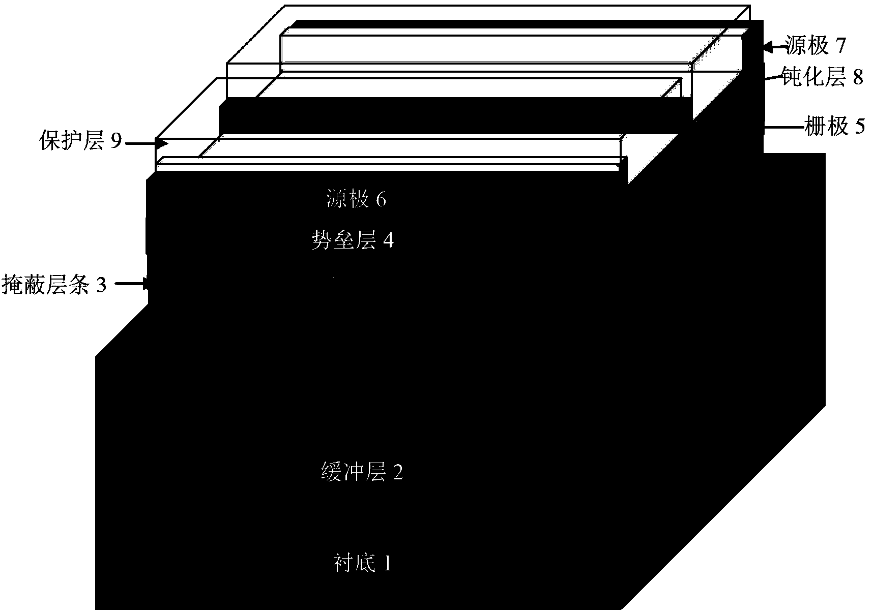
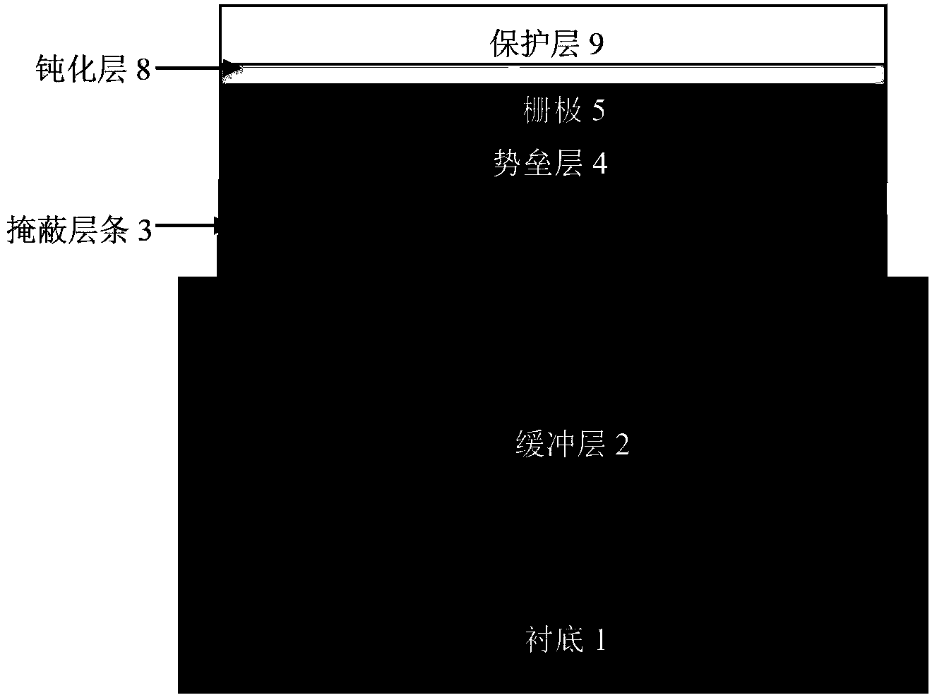
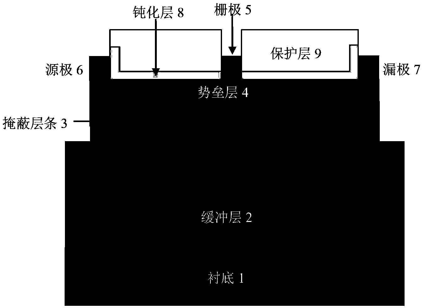
[0068] The device structure of Embodiment 1 is: substrate 1 is sapphire, buffer layer 2 is GaN, barrier layer 4 is AlGaN, passivation layer 8 is SiN, protective layer 9 is SiN, masking layer strip 3 is SiN, masking layer strip The thickness of 3 is 10nm, the width is 50nm, the interval between every two masking layer strips 3 is 10nm, and the masking layer strips 3 are arranged periodically;

Embodiment 2

[0069] The device structure of Example 2 is: the substrate 1 is silicon carbide, the buffer layer 2 is GaN, the barrier layer 4 is AlGaN, the passivation layer 8 is SiN, and the protective layer 9 is SiO 2 , the masking layer strips 3 are SiN, the thickness of the masking layer strips 3 is 30nm, the width is 250nm, the interval between every two masking layer strips 3 is 50nm, and the masking layer strips 3 are arranged periodically;

Embodiment 3

[0070] The device structure of Example 3 is: the substrate 1 is silicon, the buffer layer 2 is GaN, the barrier layer 4 is AlGaN, and the passivation layer 8 is SiO 2 , the protective layer 9 is SiN, the masking layer strips 3 are SiN, the thickness of the masking layer strips 3 is 50nm, the width is 500nm, the interval between every two masking layer strips 3 is 100nm, and the masking layer strips 3 are arranged periodically ;


PUM


Abstract

The invention discloses a crosswise overgrowth one-dimensional electron gas GaN-base high electron mobility transistor (HEMT) device and a manufacturing method thereof. The device mainly solves the problem of the existing one-dimensional electron gas devices of being poor in high-temperature high-pressure characteristic, frequency characteristic and power characteristic. The device comprises a substrate, a buffering layer, a barrier layer, a passivation layer and a protective layer from the bottom to the top. Two ends of the barrier layer are a source electrode and a drain electrode respectively, the passivation layer is arranged on the barrier layer between the source electrode and the drain electrode, a grid groove is formed in the passivation layer, and a grid is arranged in the grid groove. The barrier layer is made of AlGaN. The buffering layer is made of GaN. Masking layer strips distributed according to periodicity are arranged in the buffering layer, the gap between every two masking layer strips is in a nanometer order, and one-dimensional electron gas is formed. Compared with a Si-base and GaAs-base one-dimensional electron gas device, by adopting a wide bandgap semiconductor GaN prominent in material characteristics, the device is good in high-temperature high-pressure characteristic, frequency characteristic and power characteristic. Superspeed low-power-consumption one-dimensional electron gas devices can be manufactured.

Description

technical field [0001] The invention belongs to the technical field of microelectronics and relates to a semiconductor device, in particular a one-dimensional electron gas HEMT device based on a GaN semiconductor material heterojunction structure, which can be used as a basic device of a microwave, millimeter wave communication system and a radar system. Background technique [0002] III-V compound semiconductor materials are the third-generation semiconductor materials that have been developed rapidly for more than ten years, such as GaN-based, GaAs-based, InP-based and other semiconductor materials, which have a large band gap and can be combined with InN, AlN, etc. Alloy semiconductors are formed to make their forbidden band width adjustable. People usually use these III-V compound semiconductor materials to form various heterojunction structures. Due to the large difference in the forbidden band width of the III-V compound semiconductor materials on both sides of the het...

Claims


Application Information

Patent Timeline
Patent Type & Authority Applications(China)
IPC IPC(8): H01L29/775H01L29/20H01L29/205H01L29/06H01L21/335
Inventor 郝跃马晓华汤国平陈伟伟赵胜雷
Owner 云南凝慧电子科技有限公司
Why Eureka
Try Eureka