Chip cutting method and chip packaging method

A cutting method and chip technology, which is applied in the manufacture of electrical components, electrical solid devices, semiconductor/solid devices, etc., can solve the problems of waste of chip area, poor mechanical strength of chips, and large differences in thermal expansion coefficients, etc., to improve the integration of devices , The effect of saving chip area

Active Publication Date: 2013-11-27
NANTONG FUJITSU MICROELECTRONICS
View PDF9 Cites 19 Cited by
  • Summary
  • Abstract
  • Description
  • Claims
  • Application Information

AI Technical Summary

Problems solved by technology

[0003] However, since the three-dimensional stacking technology based on through-silicon vias needs to form several through-silicon vias in the chip, the chip needs to be thinned when forming the through-silicon vias, but the mechanical strength of the thinned chip is poor, and it is easy to deform or even break ; Simultaneously because the metal material filled in the said TSV is copper, the thermal expansion coefficient of the copper and the silicon substrate of the chip is very different, so a stress zone will be formed near the chip position of the TSV, and the stress will affect the semiconductor device Therefore, semiconductor devices cannot be formed in the stress region, which will cause a waste of chip area; at the same time, due to the high process requirements for forming through-silicon vias, the process cost is relatively high

Method used


Image

  • Chip cutting method and chip packaging method
  • Chip cutting method and chip packaging method
  • Chip cutting method and chip packaging method

Examples


Embodiment Construction

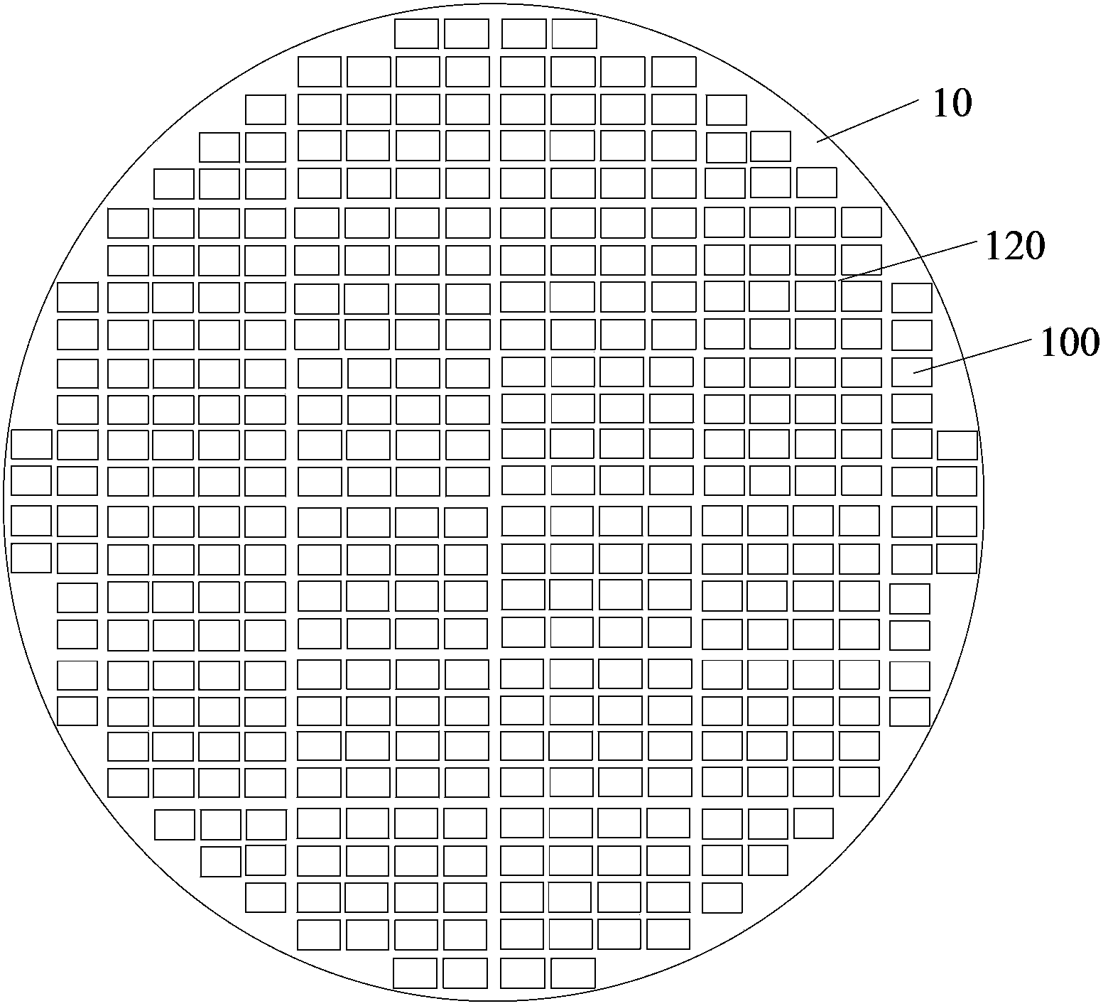
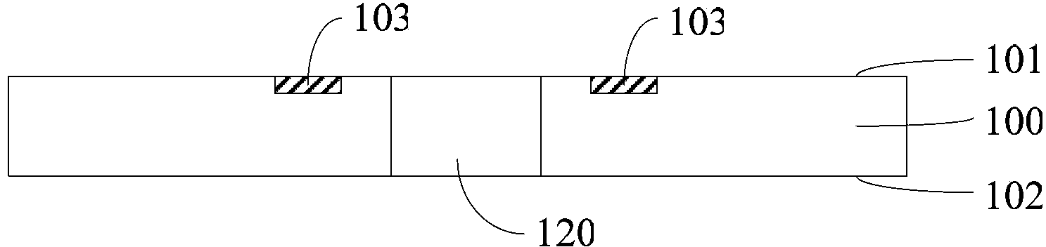
[0023] Since the process cost of the three-dimensional stacking technology based on through-silicon vias is large, it will cause waste of chip area, and the chip needs to be thinned, so that the mechanical strength of the chip will deteriorate. Therefore, the present invention provides a chip cutting method and a chip packaging method. The sidewall of the chip structure formed by the cutting method has a conductive groove. When a plurality of chip structures are stacked, the conductive groove is filled with conductive glue, and the conductive glue is used to make different chip structures The circuits are electrically connected to form a chip package structure. Since the present invention does not need to form through-silicon holes in the chip, the process of forming through-silicon holes can be saved, and the cost can be reduced; at the same time, since the conductive groove is formed on the side wall of the chip structure, only the conductive groove needs to be formed in the ...


PUM


Abstract

Provided are a chip cutting method and a chip packaging method. The chip packaging method includes the steps that at least two chip structures are provided, wherein each chip structure comprises a chip and an insulating layer at least located on the side wall of the chip, the side wall of the insulating layer of each chip structure is provided with a conductive groove, the chip structures are stacked, and the conductive grooves of the different chip structures correspond to each other in position; the insides of the conductive grooves are filled with conductive adhesives, wherein circuits in the different chip structures are electrically connected through the conductive adhesives. Due to the fact that the conductive grooves are formed in the side walls of the insulating layers, the conductive adhesives formed in the conductive grooves cannot be in direct contact with the chips, and short-circuit phenomena cannot occur; due to the fact that the conductive grooves and contact welding plates are connected through metal interconnection layers on the surfaces of the insulating layers, the insulating layers cannot influence layout design of other metal interconnection structures in the chips, the chip area occupied by the metal interconnection structures can be saved, and the component integration degree of the chips can be beneficially improved.

Description

technical field [0001] The invention relates to a semiconductor manufacturing process, in particular to a chip cutting method and a chip packaging method. Background technique [0002] With the continuous development of semiconductor technology, the feature size of semiconductor devices has become very small. It is becoming more and more difficult to increase the number of semiconductor devices in a two-dimensional chip structure. Therefore, three-dimensional packaging, that is, stacking and packaging multiple chips, has become A method that can effectively improve chip integration. Current three-dimensional packaging includes die stacking based on wire bonding, package stacking and three-dimensional stacking based on through silicon vias (Through Silicon Via, TSV). Among them, the three-dimensional stacking technology using through-silicon vias has the following three advantages: (1) high-density integration; (2) greatly shortening the length of electrical interconnections...

Claims


Application Information

Patent Timeline
Patent Type & Authority Applications(China)
IPC IPC(8): H01L21/78H01L21/60
CPCH01L24/01
Inventor 朱海青石磊王洪辉
Owner NANTONG FUJITSU MICROELECTRONICS
Why Eureka
Try Eureka