Solar cell surface passive layer structure and preparing method thereof

A technology for solar cells and passivation layers, applied in the field of solar cells, can solve the problems of high interface defect density, poor anti-reflection effect, affecting passivation effect, etc., to reduce the surface recombination rate, solve the problem of poor blocking ability, and overcome interface defects. high density effect

Inactive Publication Date: 2013-11-27
SPIC XIAN SOLAR POWER CO LTD
View PDF4 Cites 14 Cited by
  • Summary
  • Abstract
  • Description
  • Claims
  • Application Information

AI Technical Summary

Problems solved by technology

[0009] After the silicon nitride passivation film is deposited on the surface of the silicon wafer, the interface defect density is high, which affects the overall passivation effect
[0010] The refractive index of the silicon dioxide passivation film is low (about 1.46), and the anti-reflection effect on sunlight is not as good as that of the silicon nitride passivation film; and because the positive charge density of the silicon dioxide layer is very low, its field effect passivation effect is not as good as Silicon nitride passivation film is good

Method used


Image

  • Solar cell surface passive layer structure and preparing method thereof
  • Solar cell surface passive layer structure and preparing method thereof

Examples


Embodiment Construction

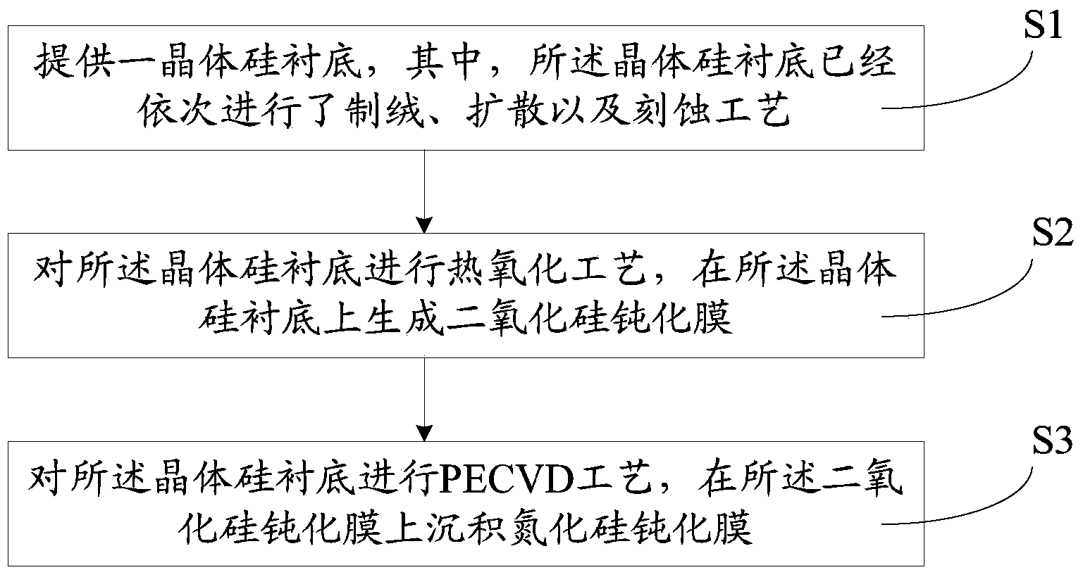
[0051] The structure of the surface passivation layer of the solar cell and the preparation method thereof provided by the present invention will be further described in detail below in conjunction with the accompanying drawings and specific embodiments. According to the following description and claims, the advantages and features of the present invention will be clearer. It should be noted that the drawings all adopt very simplified forms and all use imprecise ratios, which are only used for the purpose of conveniently and clearly assisting in describing the embodiments of the present invention.

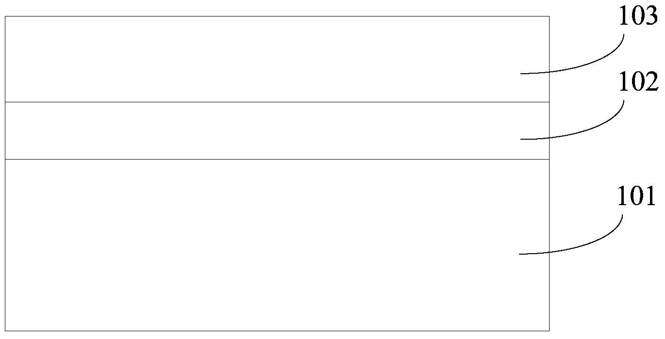
[0052] See figure 1 , figure 1 It is a schematic diagram of the structure of the passivation layer on the surface of the solar cell provided by an embodiment of the present invention, such as figure 1 As shown, the surface passivation layer structure of the solar cell provided by the present invention includes:

[0053] The silicon dioxide passivation film 102 is deposited on a crystall...


PUM

PropertyMeasurementUnit
thicknessaaaaaaaaaa
thicknessaaaaaaaaaa
thicknessaaaaaaaaaa

Abstract

The invention discloses a solar cell surface passive layer structure. A laminate passive film structure composed of a silicon dioxide passive film and a silicon nitride passive film is adopted for the structure, and therefore the defects that the interface defect density of the silicon nitride passive film is high, silicon-hydrogen bonds are not stable, the capacity for resisting metal ions of the silicon dioxide passive film is poor, moisture can be easily adsorbed and the reducing and reflecting effect of light is not good are overcome. The thickness of the silicon dioxide passive film is optimized to range from 10 nanometers to 40 nanometers, therefore, the passivating effect for electrically active impurities of silicon materials and surface defects of the silicon materials is greatly improved on the basis that the light absorbing rate is ensured, the surface recombination rate of a photon-generated carrier is obviously lowered, and the conversion efficiency of crystalline silicon can be improved by 0.3%. Meanwhile, the invention further discloses a preparing method of the solar cell surface passive layer structure. According to the method, the silicon dioxide passive film is prepared through the thermal oxidation technology, the silicon nitride passive film is prepared through the PECVD technology, and the method can be compatible with the solar cell preparing technology.

Description

Technical field [0001] The invention relates to the technical field of solar cells, in particular to a passivation layer structure on the surface of a solar cell and a preparation method thereof. Background technique [0002] Photovoltaic power generation is currently one of the main ways to use solar energy. Because of its clean, safe, convenient, and high-efficiency characteristics, solar photovoltaic power generation has become an emerging industry that is generally concerned and developed by all countries in the world. Therefore, in-depth research and utilization of solar energy resources are of great significance to alleviating the resource crisis and improving the ecological environment. [0003] Solar cell-grade silicon materials contain a large number of impurities and defects, and there are many unsaturated dangling bonds on the surface of silicon materials. The minority carrier recombination caused by these factors limits the further improvement of the conversion efficien...

Claims


Application Information

Patent Timeline
Patent Type & Authority Applications(China)
IPC IPC(8): H01L31/0216H01L31/18
CPCY02P70/50
Inventor 董鹏屈小勇张治王涛
Owner SPIC XIAN SOLAR POWER CO LTD
Why Eureka
Try Eureka