Optical processing system and method

A technology of optical processing and optical system, which is applied in the field of lithography, and can solve problems such as difficulty in realization, difficulty in making microlenses and zone plates, and high requirements for alignment adjustment accuracy of microlenses and zone plates with projection imaging systems , to achieve high energy utilization, high resolution, and improved lithography resolution

Inactive Publication Date: 2013-12-04
SUZHOU UNIV
View PDF6 Cites 12 Cited by
  • Summary
  • Abstract
  • Description
  • Claims
  • Application Information

AI Technical Summary

Problems solved by technology

This has been achieved by liquid immersion lithography and cannot be further improved
The second is to increase the aperture angle sinθ, the difficulty lies in the design and manufacture of the lens
The maximum numerical aperture of ordinary projection imaging lens can reach more than 0.75, and the maximum numerical aperture of the introduced microlens and zone plate is about 0.95 (diffractive optics for maskless lithography and imaging (P71)), and the resolution improvement is less than 30%;2 1. It is difficult to manufacture microlenses and zone plates with high numerical aperture arrays; 3. The alignment adjustment accuracy of microlenses and zone plates with the projection imaging system is very high, not only to achieve precise alignment of the X-Y array in the horizontal plane , but also to achieve the alignment of the focal plane in the height direction, it is difficult to achieve

Method used


Image

  • Optical processing system and method
  • Optical processing system and method
  • Optical processing system and method

Examples


Embodiment Construction

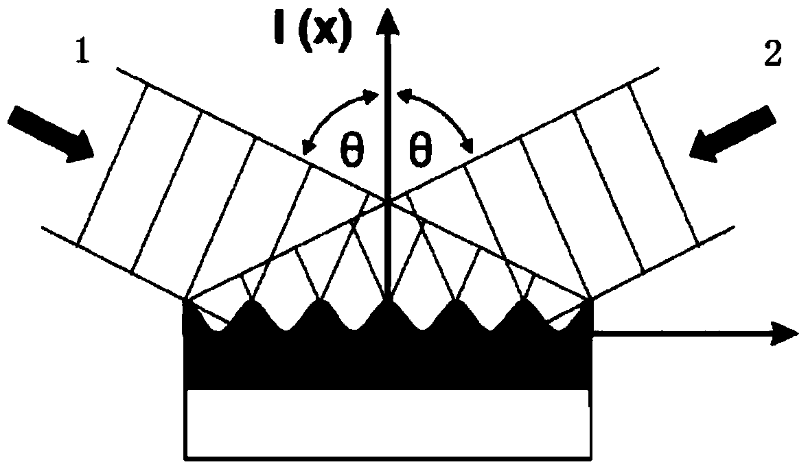
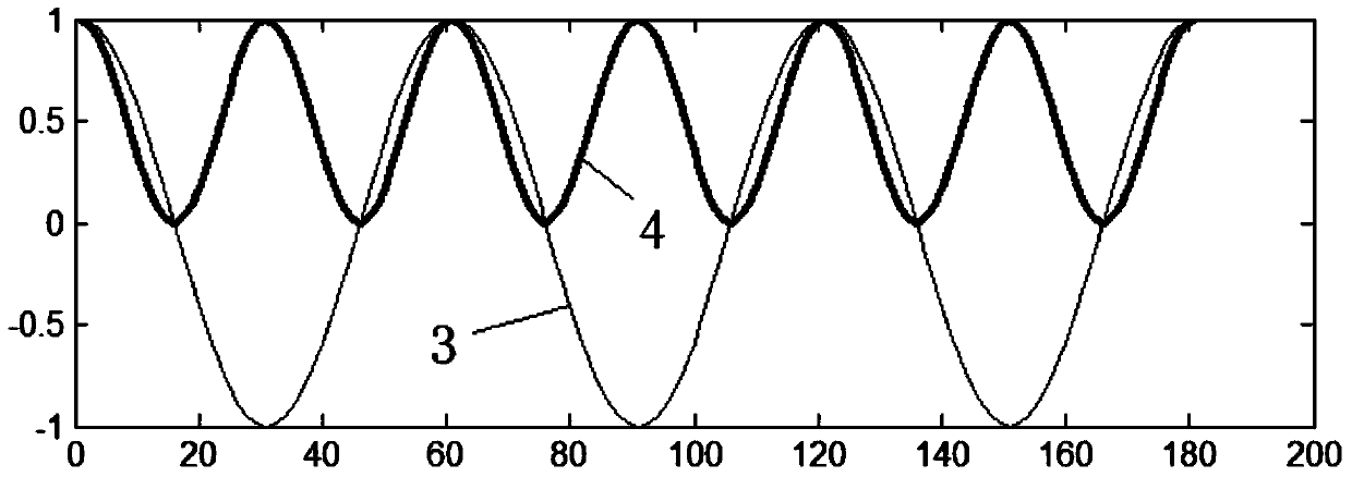
[0058] As mentioned in the background art, in the existing photolithography process, the resolution of the laser direct writing technology is limited by the wavelength of the light wave and the numerical aperture, and there is little room for improvement. Although the interference lithography technology can double the resolution of the laser direct writing technology, but because the etched image can only be an interference pattern, such as vertical stripes or periodic lattices with alternating light and dark, it is difficult to Use graphics with a high degree of freedom.

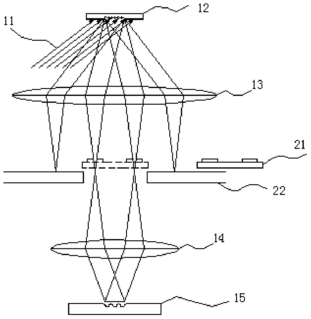
[0059] Therefore, the object of the present invention is to propose an optical processing system and method, which combines the advantages of laser direct writing technology and interference lithography technology, that is, it can pixelate the exposure pattern, thereby exposing any pattern , and can use interference lithography to improve the resolution of the exposure pattern. The optical processing syste...


PUM

PropertyMeasurementUnit
angle of incidenceaaaaaaaaaa
diameteraaaaaaaaaa

Abstract

The invention discloses an optical processing system and method. The optical processing system comprises an optical system, a bearing platform, a driving system and a control system. The optical system comprises a spatial light modulator which is used as a pattern generation device of the optical system, the spatial light modulator is provided with a plurality of pixel units, and each pixel is a reflector. When the spatial light modulator generates a pattern, the reflectors of the pixel units which establish the pattern uniformly turn over by the same angle gamma to enable the spatial light modulator to form a grating structure with gamma as a blaze angle, the grating structure conducts light diffraction and light split on incident light to enable the optical system to obtain at least two coherent light beams which can form interference, the optical system accomplishes interference direct writing combined photoetching by means of the coherent light, and therefore the distinguishability of the ordinary laser direct writing technology is greatly improved.

Description

technical field [0001] The invention relates to the technical field of photolithography, in particular to an optical processing system and method combining interference photolithography technology and laser direct writing technology. Background technique [0002] Lithography technology is a supporting technology for micro-nano manufacturing, and its application fields widely cover many industries such as microelectronics, micro-nano optics, flat panel display and biomedicine. In emerging industries, lithography technology is regarded as an indispensable technical means in the research process of new materials and new devices, and there are urgent requirements for further improvement of lithography technology, including lithography resolution, lithography quality and Efficiency of photolithographic processing. [0003] The basic principle of lithography technology is: using the miniaturization imaging optical path, the graphics on the mask plate or spatial light modulator ar...

Claims


Application Information

Patent Timeline
Patent Type & Authority Applications(China)
IPC IPC(8): G03F7/20
CPCG03F7/70291
Inventor 胡进浦东林陈林森
Owner SUZHOU UNIV
Why Eureka
Try Eureka