Method of dicing semiconductor wafer, and dicing tape for processing semiconductor using the same

A cutting method and semiconductor technology, applied in semiconductor/solid-state device manufacturing, stone processing equipment, fine working devices, etc., can solve problems such as complicated procedures, inability to remove support parts, and decreased adhesive force of semiconductor wafers with dicing tape

Active Publication Date: 2013-12-04
FURUKAWA ELECTRIC CO LTD
View PDF12 Cites 9 Cited by
  • Summary
  • Abstract
  • Description
  • Claims
  • Application Information

AI Technical Summary

Problems solved by technology

[0009] However, the process of the above-mentioned method is relatively complicated, and it is necessary to replace the dicing tape, etc. In addition, it also requires a long time of treatment to diffuse the chemical in the bonding agent, and does not solve the problems in the above-mentioned Patent Document 1. Furthermore, irradiation of ultraviolet light will cause a decrease in the adhesive force of the dicing tape relative to the semiconductor wafer. Therefore, as in Patent Document 2 and Patent Document 3, in the case of the process of mechanically peeling the support member from the semiconductor wafer, sometimes the The problem arises that peeling occurs between the semiconductor wafer-adhesive tape, not between the support member-semiconductor wafer, and the support member cannot be removed
In addition, even if the support member can be removed, there is a problem of insufficient adhesive force at the time of dicing, causing chips to fly

Method used


Image

  • Method of dicing semiconductor wafer, and dicing tape for processing semiconductor using the same
  • Method of dicing semiconductor wafer, and dicing tape for processing semiconductor using the same
  • Method of dicing semiconductor wafer, and dicing tape for processing semiconductor using the same

Examples


no. 1 Embodiment approach

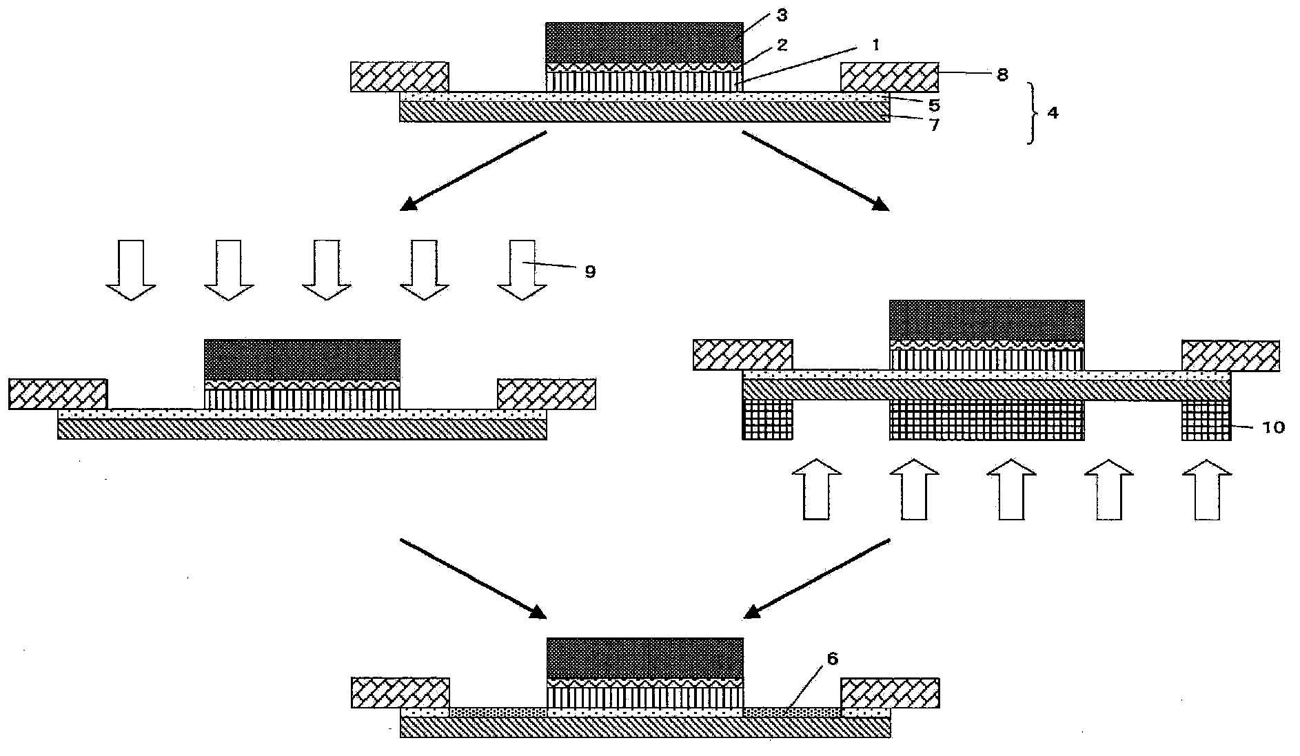
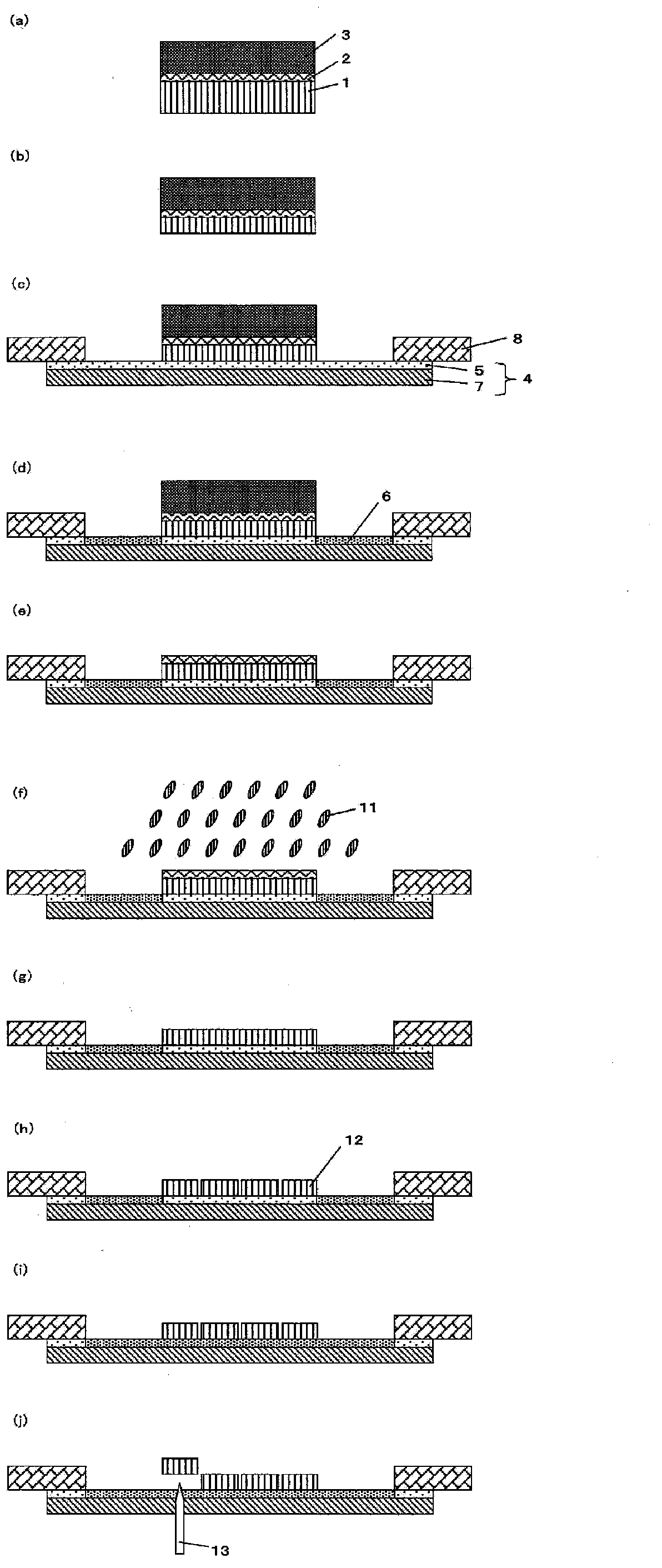
[0054] First, while referring to Figure 1~3 , while describing the first embodiment of the semiconductor wafer processing method (dicing method) of the present invention.

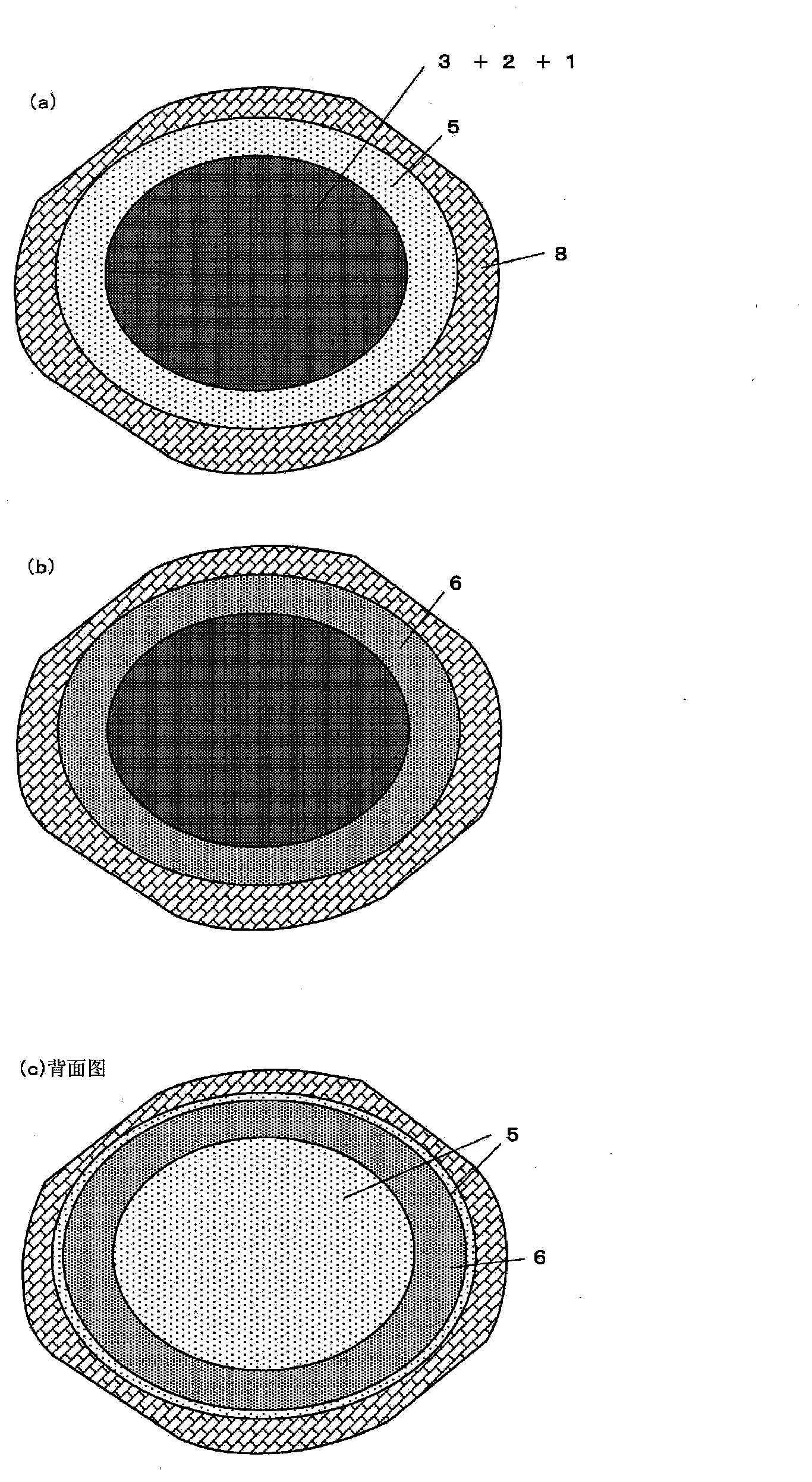
[0055] figure 1 It is a schematic sectional view showing the processing method of the semiconductor wafer 1 according to the first embodiment; figure 2 It is an overall process diagram, which is a cross-sectional view of the semiconductor wafer 1 fixed on the ring frame (dicing frame) 8 .

[0056] The semiconductor wafer 1 of the present invention is a silicon wafer or the like having a pattern surface (not shown) on which a circuit or the like is formed on one side, and a support member 3 is bonded to the circuit surface side via an adhesive (adhesive layer) 2 [ figure 2 (a)] After that, it is supplied to the back grinding (Back Grind) process [ figure 2 (b)].

[0057] After the back grinding (Back Grind) process is finished, on the back of the circuit surface of the semiconductor wafer 1, stick th...

no. 2 Embodiment approach

[0065] First, while referring to Figure 4 and Figure 5 A second embodiment of the processing method (dicing method) of the semiconductor wafer 1 of the present invention will be described.

[0066] Figure 4 It is a schematic sectional view of the dicing tape (dicing tape for semiconductor processing) 14 of the second embodiment; Figure 5 It is an overall process view of the second embodiment, and is a schematic cross-sectional view illustrating a method of processing the semiconductor wafer 1 .

[0067] Dicing tape of the present invention (dicing tape for semiconductor processing) 14[ Figure 4 (a)] is a dicing tape for semiconductor processing in which an adhesive layer is formed on at least one surface of a base film (base resin film) 7, the adhesive layer is a radiation-curable adhesive layer, and The adhesive layer in the region where the semiconductor wafer 1 and the ring frame (dicing frame) 8 are not bonded is cured by ultraviolet irradiation in advance.

[00...

Embodiment 1

[0148] For each dicing tape (C1 to C5), the PET film was peeled off from the dicing tape, and the UV-curable adhesive layer of the dicing tape was attached to the semiconductor wafer and the ring frame, and then, under a nitrogen atmosphere, from the semiconductor wafer side An evaluation sample was prepared by irradiating with ultraviolet rays to cure the adhesive layer in the region where the semiconductor wafer was not bonded in advance.


PUM

PropertyMeasurementUnit
thicknessaaaaaaaaaa
glass transition temperatureaaaaaaaaaa
thicknessaaaaaaaaaa

Abstract

The invention provides a method of dicing a semiconductor wafer and a dicing tape for semiconductor processing. The method of dicing semiconductor wafer comprises the steps of: (a) adhering a supporting member via an adhesive onto the circuit surface side of the semiconductor wafer; (b) thinning the back surface of the wafer opposite to the circuit surface side; (c) adhering a dicing tape provided with at least an ultraviolet-curable adhesive layer onto the back surface of the wafer opposite to the circuit surface side; (d) peeling the wafer from the adhesive layer and the supporting member; (e) using an organic solvent to clean the adhesive residues on the semiconductor wafer; and (f) dicing the semiconductor wafer into several chips, wherein the adhesive layer on the region of the dicing tape that is not adhered onto the semiconductor wafer is already cured by the ultraviolet irradiation prior to the above step (e).

Description

technical field [0001] The present invention relates to a method for dicing a semiconductor wafer in a manufacturing process of a semiconductor device, and a dicing tape for semiconductor processing used in the method. In more detail, this invention relates to the dicing method of a semiconductor wafer in the manufacturing process of the semiconductor element using a support member, and the dicing tape for semiconductor processing used for this method. Background technique [0002] When flaking the back surface of a semiconductor wafer on which a wiring pattern is formed, in order to protect the pattern surface of the semiconductor wafer and fix the semiconductor wafer itself, generally after attaching a protective sheet to the pattern surface, the back surface is subjected to grinding, lapping, etc. chemical processing. As such a protective sheet, a sheet obtained by coating an acrylic adhesive or the like on a base material made of a plastic film is generally used. Howev...

Claims


Application Information

Patent Timeline
Patent Type & Authority Applications(China)
IPC IPC(8): H01L21/304H01L21/683B28D5/04
CPCH01L21/6836H01L21/78
Inventor 玉川有理大田乡史矢吹朗服部聪
Owner FURUKAWA ELECTRIC CO LTD
Why Eureka
Try Eureka