Organic light-emitting device and preparation method thereof

An electroluminescent device and electroluminescent technology, which are applied in the fields of electro-solid devices, semiconductor/solid-state device manufacturing, electrical components, etc., can solve the problems of affecting luminous efficiency, low luminous efficiency of light-emitting devices, and reduced probability.

Inactive Publication Date: 2013-12-04
OCEANS KING LIGHTING SCI&TECH CO LTD +1
View PDF6 Cites 0 Cited by
  • Summary
  • Abstract
  • Description
  • Claims
  • Application Information

AI Technical Summary

Problems solved by technology

[0004] In traditional light-emitting devices, the ITO glass substrate is generally used as the light-emitting surface. In this structure, the light is first absorbed and reflected by the ITO conductive material, and then absorbed and reflected by the glass, and finally can be emitted to the air. However, because the glass surface is relatively flat and the thickness of the glass is relatively large, the optical path is increased, so that more light is refracted to both sides of the glass, resulting in a decrease in the probability of light exiting the glass to the device, which ultimately affects the luminous efficiency.
Therefore, the emission rate of light emitted into the air is very low, most of the light is lost, and the luminous efficiency of such light-emitting devices is low.

Method used


Image

  • Organic light-emitting device and preparation method thereof
  • Organic light-emitting device and preparation method thereof

Examples


Embodiment 1

[0074] A method for preparing an organic electroluminescent device, comprising the following steps:

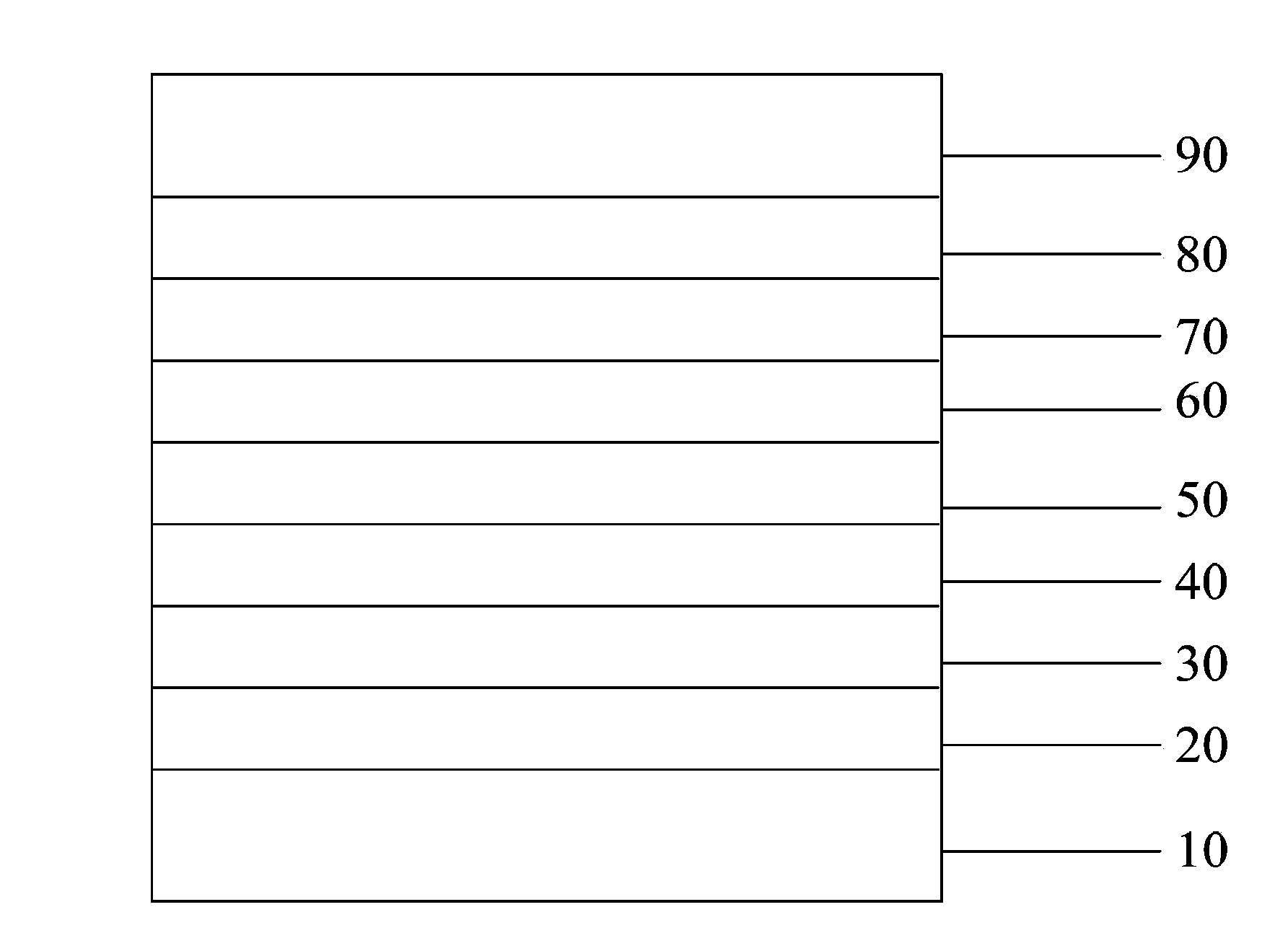
[0075] (1) Wash the glass substrate with detergent, deionized water, and ultrasonic for 15 minutes to remove organic pollutants on the glass surface; scrape the glass substrate to prepare a scattering layer, and then put it in an oven to dry the water.

[0076] Specifically, in this embodiment, the material of the scattering layer is a mixed material formed by doping carbon aerogel with a polytetrafluoroethylene (PTFE) aqueous solution with a mass fraction of 40%, wherein the doping mass fraction of the carbon aerogel The pore size of the carbon airgel is 120nm; the thickness of the scattering layer is 50μm.

[0077] (2) Prepare an anode conductive film on the scattering layer by magnetron sputtering;

[0078] Specifically, during the magnetron sputtering process, the vacuum degree is 4×10 -3 Pa, the sputtering power is 150W, and the material of the anode conductive film is ...

Embodiment 2

[0086] A method for preparing an organic electroluminescent device, comprising the following steps:

[0087] (1) Wash the glass substrate with detergent, deionized water, and ultrasonic for 15 minutes to remove organic pollutants on the glass surface; spin-coat the glass substrate to prepare a scattering layer, and then put it in an oven to dry the water.

[0088]Specifically, in this embodiment, the material of the scattering layer is a mixed material formed by doping carbon aerogel with a polytetrafluoroethylene (PTFE) aqueous solution with a mass fraction of 60%, wherein the doping mass fraction of the carbon aerogel The pore size of the carbon airgel is 20nm; the thickness of the scattering layer is 200μm. During the spin coating process, the rotational speed was 500 rpm, and the time was 15 s.

[0089] (2) Prepare an anode conductive film on the scattering layer by magnetron sputtering;

[0090] Specifically, during the magnetron sputtering process, the vacuum degree is...

Embodiment 3

[0096] A method for preparing an organic electroluminescent device, comprising the following steps:

[0097] (1) Wash the glass substrate with detergent, deionized water, and ultrasonic for 15 minutes to remove organic pollutants on the glass surface; spin-coat the glass substrate to prepare a scattering layer, and then put it in an oven to dry the water.

[0098] Specifically, in this embodiment, the material of the scattering layer is a mixed material formed by doping carbon aerogel with a polytetrafluoroethylene (PTFE) aqueous solution with a mass fraction of 20%, wherein the doping mass fraction of the carbon aerogel The pore size of the carbon airgel is 200nm; the thickness of the scattering layer is 200μm. During the spin coating process, the rotational speed was 3000 rpm and the time was 20 s.

[0099] (2) Prepare an anode conductive film on the scattering layer by magnetron sputtering;

[0100] Specifically, during the magnetron sputtering process, the vacuum degree ...


PUM


Abstract

An embodiment of the invention discloses an organic light-emitting device. The organic light-emitting device sequentially comprises a glass substrate, a scattering layer, an anode conducting film, a hole injection layer, a hole transport layer, a light-emitting layer, an electron transport layer, an electron injection layer and a cathode. The scattering layer is made of a mixed material formed by polytetrafluoroethylene water solution doped with carbon aerogel, and the doping mass fraction of carbon aerogel in the scattering layer is 5-20%. In addition, the embodiment of the invention further discloses a preparation method of the organic light-emitting device. According to the organic light-emitting device, by enabling the glass substrate to be coated with the scattering layer, the refractive index gap between the glass substrate and the anode conducting film is effectively reduced, total reflection effect of light is weakened, the light out rate is improved, light loss on the side is avoided simultaneously, and luminous efficiency is enhanced.

Description

technical field [0001] The invention relates to the related field of electronic devices, in particular to an organic electroluminescent device and a preparation method thereof. Background technique [0002] In 1987, C.W.Tang and Van Slyke of Eastman Kodak Company in the United States reported a breakthrough in the research of organic electroluminescence. A high-brightness, high-efficiency double-layer organic electroluminescent device (OLED) has been prepared using ultra-thin film technology. In this double-layer structure device, the brightness reaches 1000cd / m at 10V 2 , its luminous efficiency is 1.51lm / W, and its lifespan is more than 100 hours. [0003] The principle of OLED light emission is based on the action of an external electric field, electrons are injected from the cathode to the lowest unoccupied molecular orbital (LUMO) of organic matter, and holes are injected from the anode to the highest occupied orbital (HOMO) of organic matter. Electrons and holes mee...

Claims


Application Information

Patent Timeline
Patent Type & Authority Applications(China)
IPC IPC(8): H01L51/52H01L51/54
Inventor 周明杰王平黄辉陈吉星
Owner OCEANS KING LIGHTING SCI&TECH CO LTD
Why Eureka
Try Eureka