Chip-grade LED (Light Emitting Diode) packaging device with controllable light emitting angle and packaging process

A technology of LED packaging and lighting angle, which is applied in the direction of semiconductor devices, electrical components, circuits, etc., can solve the problems of reducing device luminous efficiency, uneven light color in space, and hidden dangers in reliability, so as to reduce the risk of chip cracking and reduce diffusion Area, the effect of improving mechanical properties

Inactive Publication Date: 2017-05-31
WUHU JUFEI PHOTOELECTRIC TECH CO LTD
View PDF4 Cites 9 Cited by
  • Summary
  • Abstract
  • Description
  • Claims
  • Application Information

AI Technical Summary

Problems solved by technology

This structure has the following problems (1) the large luminous angle is not conducive to the design of secondary optics, and the extraction rate of light is relatively low during secondary optics design; (2) the phosphor is an opaque micron-sized solid particle, which is mixed in glue Among them, at the contact with the surface of the chip, bubbles are easy to form around the phosphor particles, which affects the adhesion between the adhesive layer and the chip, and the phosphor particles have a back reflection effect on light, which affects the extraction rate of blue light and fluorescence, and reduces the light extraction efficiency; The refractive index of the glue in the fluorescent glue is generally 1.4-1.54, while the LED chip sapphire has a refractive index of 1.78. The refractive index difference between the two is

Method used


Image

  • Chip-grade LED (Light Emitting Diode) packaging device with controllable light emitting angle and packaging process
  • Chip-grade LED (Light Emitting Diode) packaging device with controllable light emitting angle and packaging process
  • Chip-grade LED (Light Emitting Diode) packaging device with controllable light emitting angle and packaging process

Examples


Embodiment 1

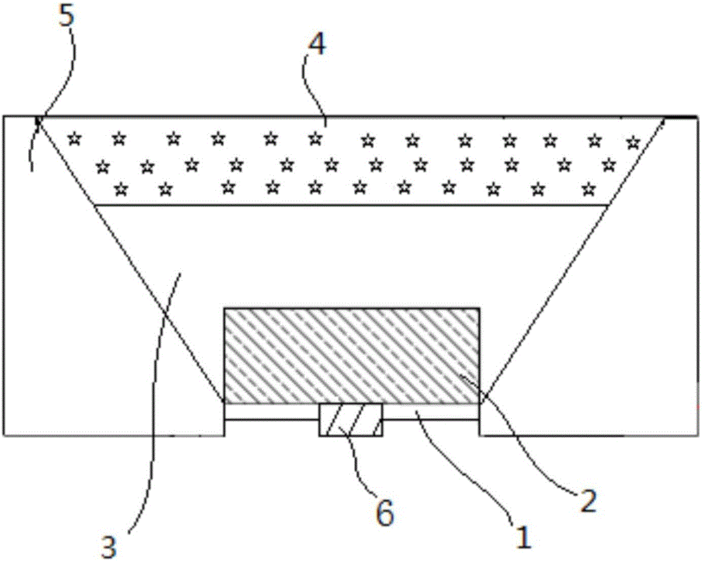
[0035] This embodiment provides a chip-level LED packaging device with controllable luminous angle, such as figure 1As shown, it includes a sapphire LED chip 2 with an electrode 1 on the bottom surface, the electrode 1 is composed of a positive electrode and a negative electrode, there is a gap between the positive electrode and the negative electrode, and a diffusion layer 3 is provided on the top and side of the LED chip 2 , the diffusion layer 3 is located above the electrode 1, the top of the diffusion layer 3 is provided with a fluorescent adhesive layer 4, and the sides of the LED chip 2, the diffusion layer 3, and the fluorescent adhesive layer 4 are provided with a first white wall glue layer 5 , the refractive index of the LED chip 2 is greater than the refractive index of the diffusion layer 3 , and the refractive index of the diffusion layer 3 is greater than the refractive index of the fluorescent glue layer 4 . In this embodiment, the LED chip 2 is a sapphire chip...

Embodiment 2

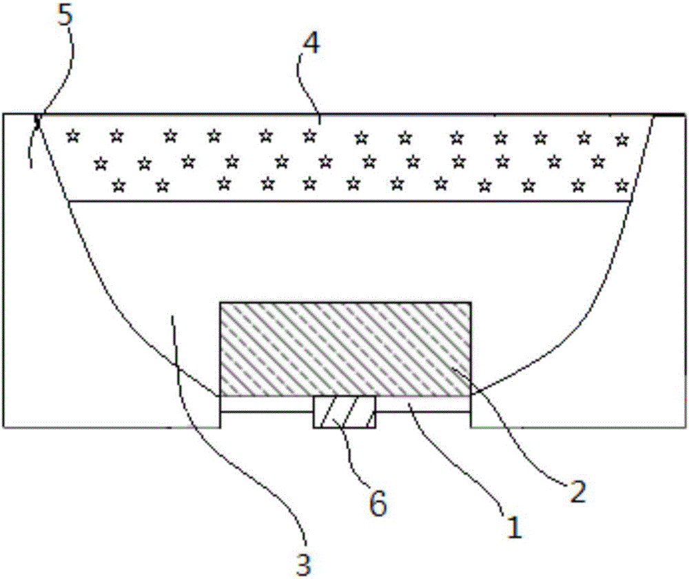
[0048] This embodiment provides a chip-level LED packaging device with controllable luminous angle, such as figure 2 As shown, it includes a sapphire LED chip 2 with an electrode 1 on the bottom surface, the electrode 1 is composed of a positive electrode and a negative electrode, there is a gap between the positive electrode and the negative electrode, and a diffusion layer 3 is provided on the top and side of the LED chip 2 , the diffusion layer 3 is located above the electrode 1, the top of the diffusion layer 3 is provided with a fluorescent adhesive layer 4, and the sides of the LED chip 2, the diffusion layer 3, and the fluorescent adhesive layer 4 are provided with a first white wall glue layer 5 , the refractive index of the LED chip 2 is greater than the refractive index of the diffusion layer 3 , and the refractive index of the diffusion layer 3 is greater than the refractive index of the fluorescent glue layer 4 . In this embodiment, the LED chip 2 is a sapphire ch...

Embodiment 3

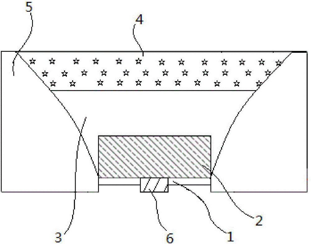
[0061] This embodiment provides a chip-level LED packaging device with controllable luminous angle, such as image 3 As shown, it includes a sapphire LED chip 2 with an electrode 1 on the bottom surface, the electrode 1 is composed of a positive electrode and a negative electrode, there is a gap between the positive electrode and the negative electrode, and a diffusion layer 3 is provided on the top and side of the LED chip 2 , the diffusion layer 3 is located above the electrode 1, the top of the diffusion layer 3 is provided with a fluorescent adhesive layer 4, and the sides of the LED chip 2, the diffusion layer 3, and the fluorescent adhesive layer 4 are provided with a first white wall glue layer 5 , the refractive index of the LED chip 2 is greater than the refractive index of the diffusion layer 3 , and the refractive index of the diffusion layer 3 is greater than the refractive index of the fluorescent glue layer 4 . In this embodiment, the LED chip 2 is a sapphire chi...


PUM

PropertyMeasurementUnit
Thicknessaaaaaaaaaa
Thicknessaaaaaaaaaa
Thicknessaaaaaaaaaa

Abstract

The invention discloses a chip-grade LED (Light Emitting Diode) packaging device with a controllable light emitting angle and a packaging process. According to the LED packaging device, first white wall adhesive layers are arranged on side faces of an LED chip, a diffusion layer and a fluorescent adhesive layer and are used as reflection surfaces; the reflection surfaces with different shapes can be designed aiming at requirements on different light emitting angles, so that the LED packaging device with the controllable light emitting angle is obtained; furthermore, the diffusion layer is arranged between the LED chip and the fluorescent adhesive layer, and the diffusion layer has a refractive index higher than that of a fluorescent adhesive; the difference between the refractive indexes of the LED chip and the fluorescent adhesive layer is reduced; the refractive indexes of the LED chip, the diffusion layer and the fluorescent adhesive layer have a certain gradient and the light emitting efficiency of the LED chip is improved, so that the luminous flux of the device is improved; the refractive indexes of diffusion powder and a packaging adhesive in the diffusion layer are different, and the condition that light emission of blue light of the LED chip is not uniform can be improved, so that the space color uniformity of the device is improved; and the design of a concave groove and white wall structure is adopted, so that the reliability problem of a product is greatly improved.

Description

technical field [0001] The invention belongs to the technical field of LED packaging, and relates to a chip-level LED packaging device, in particular to a chip-level LED packaging device and a packaging process with a controllable luminous angle. Background technique [0002] In recent years, under the trend of global energy saving and emission reduction, LED light sources have developed rapidly. Compared with traditional light sources, LED light sources have the advantages of long life, small size, high efficiency, fast response, shock resistance, energy saving, and no pollution. , is a "green light source", and LED light sources are bound to be used on a large scale. [0003] In the production process of LED light sources, packaging is a key link between the past and the future. The function of packaging is to provide sufficient protection for the light-emitting chip, preventing the chip from being exposed to aging in the air for a long time or being damaged by mechanical ...

Claims


Application Information

Patent Timeline
IPC IPC(8): H01L33/48H01L33/58H01L33/60H01L33/54H01L33/56
CPCH01L33/486H01L33/54H01L33/56H01L33/58H01L33/60H01L2933/0091
Inventor 龚涛张志宽
Owner WUHU JUFEI PHOTOELECTRIC TECH CO LTD
Why Eureka
Try Eureka