Manufacturing method of quantum dot light-emitting component and quantum dot displaying device

A technology of quantum dot light-emitting and manufacturing methods, which is applied in semiconductor/solid-state device manufacturing, electrical components, semiconductor devices, etc., can solve the problems of complex processes, many processes for quantum dot light-emitting components, and difficulty in reducing manufacturing costs, and simplify the manufacturing process. , The effect of improving the dissolution problem and reducing the manufacturing cost

Active Publication Date: 2013-12-04
BOE TECH GRP CO LTD
View PDF3 Cites 28 Cited by
  • Summary
  • Abstract
  • Description
  • Claims
  • Application Information

AI Technical Summary

Problems solved by technology

[0005] In the manufacturing process of quantum dot light-emitting elements in the prior art, the structure of each layer of the quantum dot light-emitting layer is realized in a step-by-step or layer-by-layer manner, and the quantum dot light-emitting layer is usually formed on the hole transport layer by a solution process. Since the solvent used to form the quantum dot light-emitting layer will dissolve the hole transport layer components when forming the quantum dot light-emitting layer, the components of the hole transport layer below the quantum dot light-emitting layer are also dissolved, so it is necessary to select Materials that cannot be dissolved in the process, so the materials for preparing the hole transport layer are limited; in addition, when the above-mentioned preparation method is used, the quantum dot light-emitting element has many procedures and complicated processes, which makes it difficult to reduce the manufacturing cost

Method used


Image

  • Manufacturing method of quantum dot light-emitting component and quantum dot displaying device
  • Manufacturing method of quantum dot light-emitting component and quantum dot displaying device
  • Manufacturing method of quantum dot light-emitting component and quantum dot displaying device

Examples


preparation example Construction

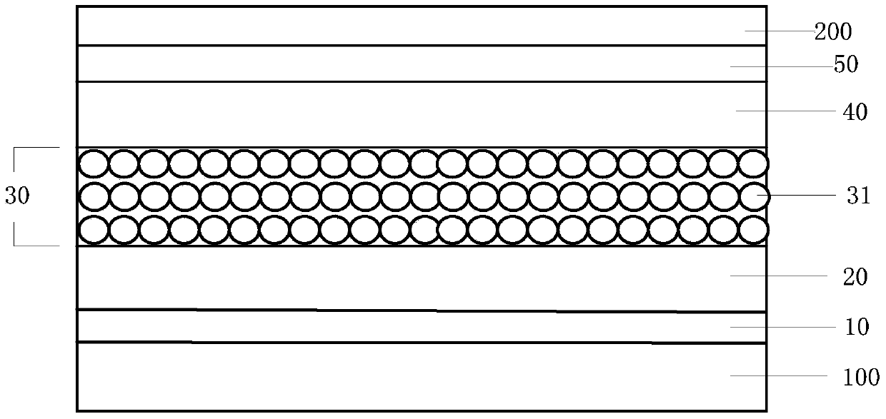
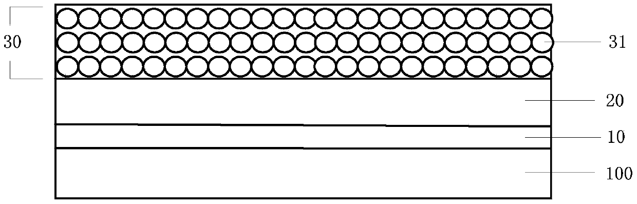
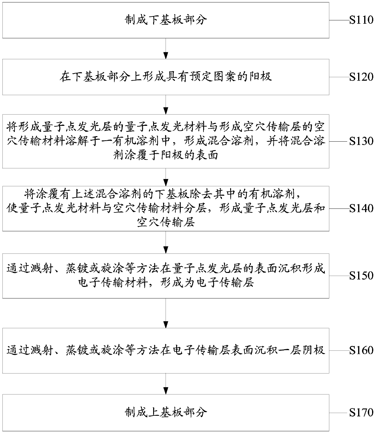
[0055] removing the organic solvent on the prepared substrate coated with the mixed solvent, layering the quantum dot luminescent material and the hole transport material or the quantum dot luminescent material and the electron transport material forming the electron transport layer on the prepared substrate, Forming the quantum dot light emitting layer and the hole transport layer or forming the quantum dot light emitting layer and the electron transport layer.

[0056] Using the above method, the quantum dot light-emitting layer and the hole transport layer (or the electron transport layer) can be formed through a one-step process without further layered manufacturing, thus simplifying the manufacturing process of the quantum dot light-emitting element, The manufacturing cost of the quantum dot light-emitting element can be further reduced.

[0057] In addition, the mixed solvent can be formed on the prepared substrate by common solution coating processes such as spin coatin...


PUM

PropertyMeasurementUnit
sizeaaaaaaaaaa
sizeaaaaaaaaaa

Abstract

The invention provides a manufacturing method of a quantum dot light-emitting component and a quantum dot displaying device. The quantum dot light-emitting component comprises a quantum dot luminous layer, a hole transferring layer and an electron transferring layer. The manufacturing method includes mixing quantum dot light-emitting materials with hole transferring materials, or mixing quantum dot light-emitting materials with electron transferring materials to dissolve in organic solvent to prepare mixed solvent; coating the mixed solvent on a preparing substrate of the quantum dot light-emitting component; removing the organic solvent on the preparing substrate coated with the mixed solvent, separating the preparing materials of the quantum dot light-emitting materials and the hole transferring materials or the preparing materials of the quantum dot light-emitting materials and the electron transferring materials on the preparing substrate into layers to form a quantum dot light-emitting layer and a hole transferring layer or a quantum dot light-emitting layer and an electron transferring layer. With the manufacturing method of the quantum dot light-emitting component and the quantum dot displaying device, the quantum dot light-emitting layer and the hole transferring layer (or the electron transferring layer) can be manufactured in one step without being manufactured in many steps, so that manufacturing process is simplified.

Description

technical field [0001] The invention relates to the field of display technology, in particular to a method for manufacturing a quantum dot light-emitting element and a quantum dot display device. Background technique [0002] Quantum dots (Quantum Dot, QD), also known as nanocrystals, are quasi-zero-dimensional nanomaterials. The sizes of the three dimensions of quantum dots are all between 1 and 10nm, and the movement of internal electrons in all directions is limited. , so the quantum confinement effect is particularly significant. Since electrons and holes are quantum-confined, the continuous energy band structure becomes a discrete energy-level structure with molecular characteristics. For quantum dots of different sizes, the degrees of quantum confinement of electrons and holes are different, and the discrete energy level structure of molecular characteristics is also different due to the size of quantum dots. Therefore, after being excited by external energy, quantum...

Claims


Application Information

Patent Timeline
Patent Type & Authority Applications(China)
IPC IPC(8): H01L51/56H01L27/32
CPCH10K59/38H10K50/115H10K59/122H10K59/1201
Inventor 张锋姚琪惠官宝
Owner BOE TECH GRP CO LTD
Why Eureka
Try Eureka