Semiconductor device and forming method, starting circuit and switching power source of semiconductor device

A semiconductor and device technology, applied in the field of switching power supply, can solve problems such as increasing the area of ​​the control chip, and achieve the effect of reducing metal interconnection, reducing the number of ports, and saving chip area

Active Publication Date: 2013-12-11
CSMC TECH FAB2 CO LTD
View PDF4 Cites 19 Cited by
  • Summary
  • Abstract
  • Description
  • Claims
  • Application Information

AI Technical Summary

Problems solved by technology

However, this requires an increase in the area of ​​the control chip

Method used


Image

  • Semiconductor device and forming method, starting circuit and switching power source of semiconductor device
  • Semiconductor device and forming method, starting circuit and switching power source of semiconductor device
  • Semiconductor device and forming method, starting circuit and switching power source of semiconductor device

Examples


Embodiment Construction

[0060] In order to make the purpose, features and advantages of the present invention more comprehensible, specific implementations of the present invention will be described in detail below in conjunction with the accompanying drawings.

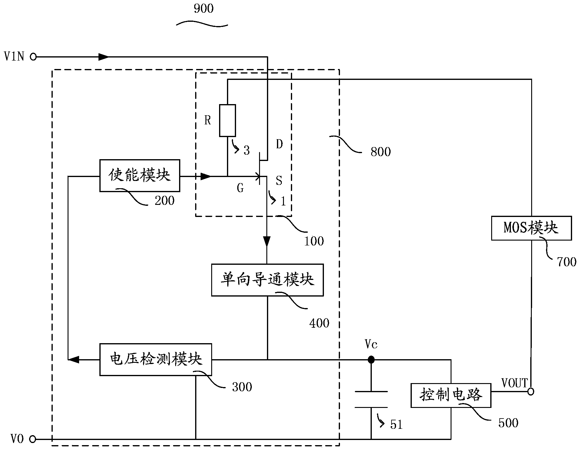
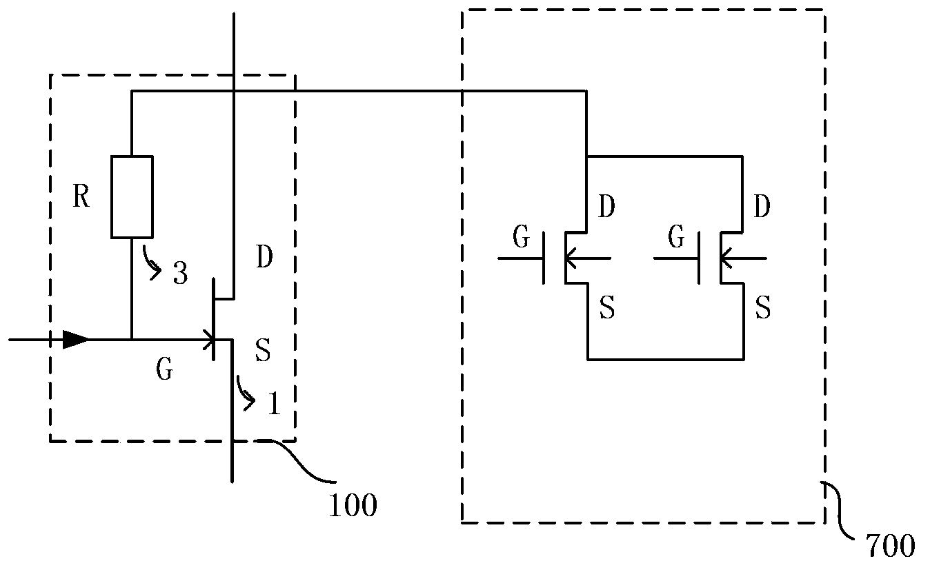
[0061] Such as figure 1 As shown, this embodiment provides a switching power supply 900, the switching power supply 900 includes a start-up circuit 800, in addition, the switching power supply 900 also includes a control circuit 500, a bypass capacitor 51 of the control circuit 500, a voltage input Terminal VIN, relative ground terminal V0 , voltage output terminal VOUT and MOS module 700 .

[0062] Wherein, one end of the control circuit 500 is connected to the relative ground terminal V0, and the other end is the voltage input terminal Vc. The bypass capacitor 51 is connected between the relative ground terminal V0 and the voltage input terminal Vc of the control circuit. The bypass capacitor 51 The voltage drop in is the voltage value in...


PUM


Abstract

The invention provides a semiconductor device and a forming method, a starting circuit and a switching power source of the semiconductor device. The switching power source comprises the starting circuit. The semiconductor device comprises a P-type semiconductor substrate, an N-type drift region, an oxide layer, an intrinsic polycrystalline silicon layer, a doping polycrystalline silicon layer and a metal plug, wherein a source electrode and a drain electrode of a negative threshold field-effect tube are arranged at the two ends of the N-type drift region, the source electrode and the drain electrode are exposed out of the oxide layer, the intrinsic polycrystalline silicon layer is arranged at one end, close to the source electrode, of the oxide layer, and the doping polycrystalline silicon layer is arranged at one end, close to the drain electrode, of the oxide layer. The intrinsic polycrystalline silicon layer and the oxide layer form a grid electrode of the negative threshold field-effect tube, the doping polycrystalline silicon layer forms a resistor connected with the grid electrode, and the metal plug is connected with the drain electrode of the negative threshold field-effect tube and is adjacent to the doping polycrystalline silicon layer. In the semiconductor device, the resistor connected with the drain electrode and the grid electrode of the negative threshold field-effect tube is formed at the position, arranged between the drain electrode and the grid electrode, of the semiconductor substrate and shares the metal plug with the drain electrode, the area of a chip is saved, metal interconnection is reduced through port sharing, and the reliability of the semiconductor device is improved.

Description

technical field [0001] The invention relates to the field of switching power supplies, in particular to a semiconductor device and its forming method, a starting circuit and a switching power supply including the starting circuit. Background technique [0002] Currently, switching power supply circuits use PWM (pulse width modulation) control chips to control on or off. The PWM control chip generally integrates high-voltage devices to form a start-up circuit to complete the initial start-up, thereby converting the higher external input voltage into the required lower bias voltage inside the PWM chip. [0003] US Patent No. 5,581,453 discloses a starting circuit for switching power supplies. The switching power supply also includes a transformer, a switching transistor, a power control circuit and a starting circuit. The switching transistor switches the transformer for periodic connection to the input voltage. The periodic pulses driving the switching transistors are perf...

Claims


Application Information

Patent Timeline
Patent Type & Authority Applications(China)
IPC IPC(8): H01L29/78H01L21/22H02M1/36G05F1/66
Inventor 张森张广胜
Owner CSMC TECH FAB2 CO LTD
Why Eureka
Try Eureka