Method for cleaning solar cell silicon wafer after polishing

A technology for polishing solar cells and silicon wafers, which is applied in the direction of cleaning methods using liquids, cleaning methods and utensils, chemical instruments and methods, etc., which can solve problems such as efficiency reduction and leakage, and achieve good texturing effects and a wide process control window , The effect of increasing the open circuit voltage

Inactive Publication Date: 2013-12-11
昊诚光电(太仓)有限公司
View PDF8 Cites 12 Cited by
  • Summary
  • Abstract
  • Description
  • Claims
  • Application Information

AI Technical Summary

Problems solved by technology

If the cleaning is not thorough, it will cause different degrees of leakage and lead to a decrease in efficiency

Method used


Image

  • Method for cleaning solar cell silicon wafer after polishing
  • Method for cleaning solar cell silicon wafer after polishing
  • Method for cleaning solar cell silicon wafer after polishing

Examples


Embodiment 1

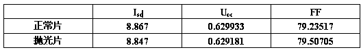
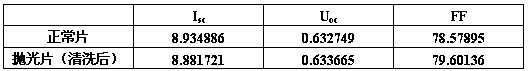
[0026] The method for cleaning solar cell silicon wafers after polishing of the present invention is used to clean the silicon wafers after polishing and before texturing, and the specific processing steps of polishing, cleaning and texturing of solar cell silicon wafers are as follows:

[0027] 1. Chemically clean the silicon wafer, and polish both sides of the silicon wafer with hot alkali.

[0028] 1. Cleaning the polished silicon wafer with hydrofluoric acid can remove the residual alkali in the polishing process.

[0029] , Perform mixed acid pickling, alkali cleaning, acid cleaning, and water washing on silicon wafers. Wherein the mixed acid adopts the mixed acid of hydrofluoric acid and nitric acid, and the volume ratio of hydrofluoric acid to nitric acid and water is 1:3:2; the sodium hydroxide solution with a mass fraction of 5% is used for alkali cleaning; then The volume fraction of the acid is 10% mixed acid of hydrofluoric acid and hydrochloric acid for a...

Embodiment 2

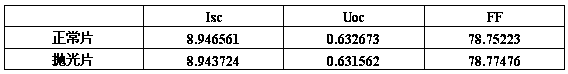
[0044] The method for cleaning solar cell silicon wafers after polishing of the present invention is used to clean the silicon wafers after polishing and before texturing, and the specific processing steps of polishing, cleaning and texturing of solar cell silicon wafers are as follows:

[0045] 1. Chemically clean silicon wafers and perform double-sided polishing process.

[0046] , Cleaning the silicon wafer with hydrofluoric acid can remove the residual alkali in the polishing process;

[0047] 3. Perform mixed acid pickling, alkali cleaning, acid cleaning, and water washing on silicon wafers. Wherein mixed acid adopts the mixed acid of hydrofluoric acid, nitric acid and sulfuric acid, and the volume ratio of hydrofluoric acid, nitric acid, sulfuric acid and water is 1:3:1:2; Then carry out alkaline cleaning with 3% potassium hydroxide solution; Then Use a mixed acid of hydrofluoric acid and hydrochloric acid with a volume fraction of 10% hydrofluoric acid for acid...


PUM


Abstract

The invention provides a method for cleaning a solar cell silicon wafer after polishing. The method includes the following steps that (1) the solar cell silicon wafer after polishing is subjected to acid cleaning, and (2) the solar cell silicon wafer after acid cleaning is subjected to mixed acid cleaning, alkali cleaning and acid cleaning. In the step (2), mixed acid of hydrofluoric acid and nitric acid is used for the mixed acid cleaning, sodium hydroxide solutions or potassium hydroxide solutions are used for the alkali cleaning, and mixed acid of hydrofluoric acid and hydrochloric acid is used for the acid cleaning. The method is simple and convenient to operate, capable of efficiently eliminating various pollutions, generated in the polishing process, of the solar cell silicon wafer, and capable of obviously improving open-circuit voltages of silicon wafer products, and good technological support is provided for mass production of back polishing cells and back passivating cells.

Description

technical field [0001] The invention relates to a method for preparing a silicon wafer of a battery, and more particularly to a method for cleaning a silicon wafer of a solar battery after polishing. Background technique [0002] Solar cells have developed from the initial immaturity to the current mature crystalline silicon cell technology. With the continuous emergence of various high-efficiency cells, not only the technology and materials are constantly being innovated, but also the technology is constantly innovating. Compared with the production process, the preparation process of the crystalline silicon solar cell structure in the back electric field area in the laboratory is not only high in production cost, but also complicated and cumbersome, and has not yet been applied to commercial production on a large scale. The main difference between the crystalline silicon battery in contact with the back electric field area and the ordinary crystalline silicon battery is th...

Claims


Application Information

Patent Timeline
Patent Type & Authority Applications(China)
IPC IPC(8): H01L31/18B08B3/00C30B33/10
CPCY02P70/50
Inventor 安子凤刘古岩牛春晓吴卫伟黄高山熊军王雅男
Owner 昊诚光电(太仓)有限公司
Why Eureka
Try Eureka