Shallow trench isolation manufacturing method and cmos manufacturing method

A shallow trench and isolation trench technology, applied in semiconductor/solid-state device manufacturing, electrical components, circuits, etc., can solve problems such as increasing leakage, reducing the threshold voltage of semiconductor devices, and the loss of the top of the oxide layer 5, and reaching a stable threshold value Voltage, performance improvement, effect of suppressing narrow channel effect

Active Publication Date: 2015-11-25
SEMICON MFG INT (SHANGHAI) CORP
View PDF2 Cites 0 Cited by
  • Summary
  • Abstract
  • Description
  • Claims
  • Application Information

AI Technical Summary

Problems solved by technology

[0004] like Figure 1c As shown, because in the existing process, during the process of removing the hard mask layer 3 and the remaining pad oxide layer 2, the top of the oxide layer 5 will also be affected by wet etching and be lost. A depression 6 will be formed at the interface between the top and the substrate; in the subsequent process of manufacturing CMOS, the substrate surface on both sides of the oxide layer 5 will be thermally oxidized to grow a gate oxide layer. Due to the influence of the shape, at the depression 6, That is, the gate oxide layer formed on the surface of the substrate 1 at the top sidewall of the shallow trench in the substrate 1 is thinner than the gate oxide layer formed on the horizontal surface, which is equivalent to forming a thin gate oxide layer at the edge of the active region. Parasitic transistors, and thus induce the narrow channel effect (Narrowwidtheffect, NWE), Burenkov&Lorenz, FraunhoferInstitut (2003), thereby reducing the threshold voltage of semiconductor devices, reducing the effective turn-on voltage of narrow channel semiconductor devices, and increasing leakage

Method used


Image

  • Shallow trench isolation manufacturing method and cmos manufacturing method
  • Shallow trench isolation manufacturing method and cmos manufacturing method
  • Shallow trench isolation manufacturing method and cmos manufacturing method

Examples


Embodiment Construction

[0033] The principles and features of the present invention are described below in conjunction with the accompanying drawings, and the examples given are only used to explain the present invention, and are not intended to limit the scope of the present invention.

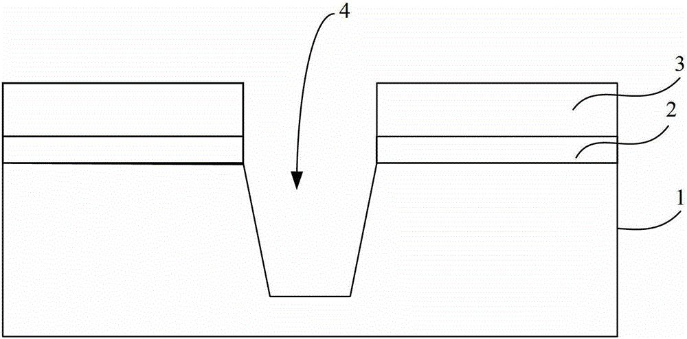
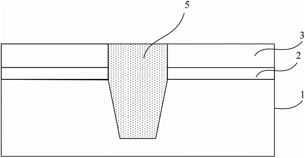
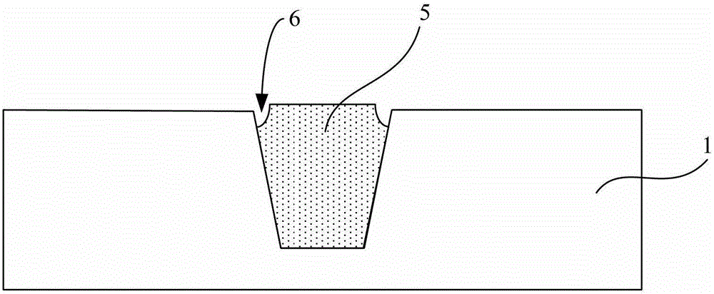
[0034] Aiming at the defects of the prior art, that is, due to the unavoidable depression at the interface between the top of the oxide filled in the shallow trench and the substrate, the formation of the gate oxide layer is affected by the morphology at this point, resulting in a thinner oxide layer. layer, and then induce the narrow channel effect, the starting point of the present invention is to increase the thickness of the oxide layer formed on the surface of the substrate in the depression, and because the region doped with fluorine ions in the substrate has a higher oxide growth rate than the The region not doped with fluorine ions, the present invention is proposed based on the above principle.

[0035] Suc...


PUM


Abstract

The invention provides an STI (shallow trench isolation) preparation method and a CMOS (complementary metal oxide semiconductor) manufacturing method. In processes of forming an STI structure, two-step oxide filling is performed, and part of a shallow trench top end side wall is exposed during primary oxide filling and is doped with fluoride ion. After the processes of forming the STI structure, the shallow trench top end side wall doped with the fluoride ion is exposed due to a recess; in the subsequent process of forming a gate oxide layer, due to influence of doping of the fluoride ion, the growth rate of oxide in a semiconductor area doped with the fluoride ion is higher than that of oxide in other area, and the oxide layer on the surface of a substrate in the recess is thicker than a gate insulator layer growing in other area. Therefore, narrow width effect is suppressed, threshold voltage of devices is stabilized, and performance of semiconductor devices is improved.

Description

technical field [0001] The present invention relates to the field of semiconductor manufacturing, in particular to a shallow trench isolation manufacturing method and a CMOS (Complementary Metal Oxide Semiconductor, Complementary Metal Oxide Semiconductor) manufacturing method. Background technique [0002] As the semiconductor process enters the deep submicron stage, in order to realize high-density, high-performance large-scale integrated circuits, the isolation process between semiconductor devices becomes more and more important. The existing technology generally adopts shallow trench isolation technology (STI, Shallow Trench Isolation) to realize the isolation of active devices, such as CMOS (ComplementaryMetalOxideSemiconductor, complementary metal oxide semiconductor) devices, NMOS (N-Mental-Oxide-Semiconductor, N-type metal The isolation layer between the oxide semiconductor) transistor and the PMOS (P-Mental-Oxide-Semiconductor, P-type metal oxide semiconductor) tra...

Claims


Application Information

Patent Timeline
Patent Type & Authority Patents(China)
IPC IPC(8): H01L21/762H01L21/8238
Inventor 刘金华
Owner SEMICON MFG INT (SHANGHAI) CORP
Why Eureka
Try Eureka