Integrated circuit packaging structure and packaging method thereof

A packaging structure and integrated circuit technology, applied in the direction of circuits, electrical components, electric solid devices, etc., can solve the problem that can not take into account device heat dissipation and air tightness at the same time. Problems such as heat dissipation methods and the inability of heat dissipation devices to establish heat dissipation channels to achieve the effect of meeting high reliability requirements, ensuring impact resistance requirements, and ensuring reliability

Active Publication Date: 2013-12-18
EAST CHINA INST OF OPTOELECTRONICS INTEGRATEDDEVICE
View PDF5 Cites 20 Cited by
  • Summary
  • Abstract
  • Description
  • Claims
  • Application Information

AI Technical Summary

Problems solved by technology

The disadvantage of this package structure is: this is a conventional airtight package design, the integration level is relatively low, the heat dissipation device cannot establish a heat dissipation channel with the shell, and the heat cannot be directly conducted to the shell
The disadvantage of this method is that the heat dissipation device is attached to the integrated circuit chip and the attachment structure to dissipate the heat, but the heat of the integrated circuit chip is not transferred out in the airtight metal tube shell.
The disadvantage of this airtight package heat dissipation structure is: this patent mainly emphasizes the design of airtight heat dissipation structure, and does not involve the heat transfer method and heat dissipation method of internal components
[0005] It can be seen that in the existing packaging technology, the packaging structure and packaging method cannot take into account both the heat dissipation of the device and the hermetic packaging.

Method used


Image

  • Integrated circuit packaging structure and packaging method thereof
  • Integrated circuit packaging structure and packaging method thereof
  • Integrated circuit packaging structure and packaging method thereof

Examples


Embodiment 1

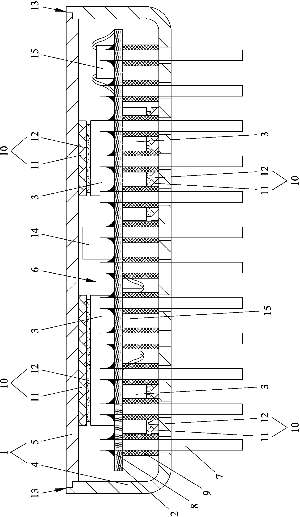
[0033] Embodiment one: see attached figure 1 shown. An integrated circuit packaging structure includes a metal casing 1 and a substrate 2 installed in the metal casing 1 and having surface mount devices 14 and bare chips 15 arranged on both sides. Substrate 2 is made of beryllium oxide, Al 2 o 3 Or PCB and other materials that can be used as circuit substrates, have a certain resistance to mechanical impact, and have the characteristics of general material selection. The surface-mount device 14 and the bare chip 15 have heat-generating devices 3 (ie, power devices) that require heat dissipation paths to be designed in the packaging structure.

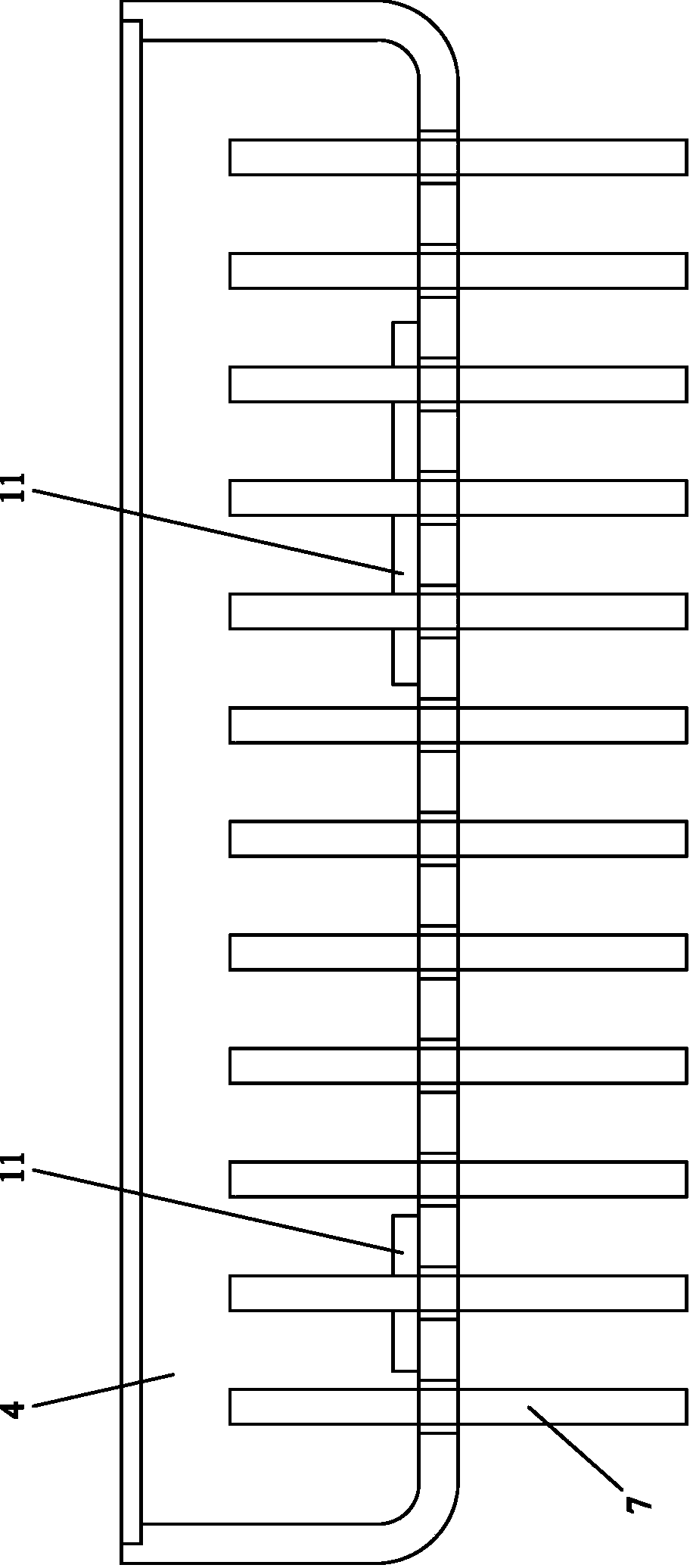
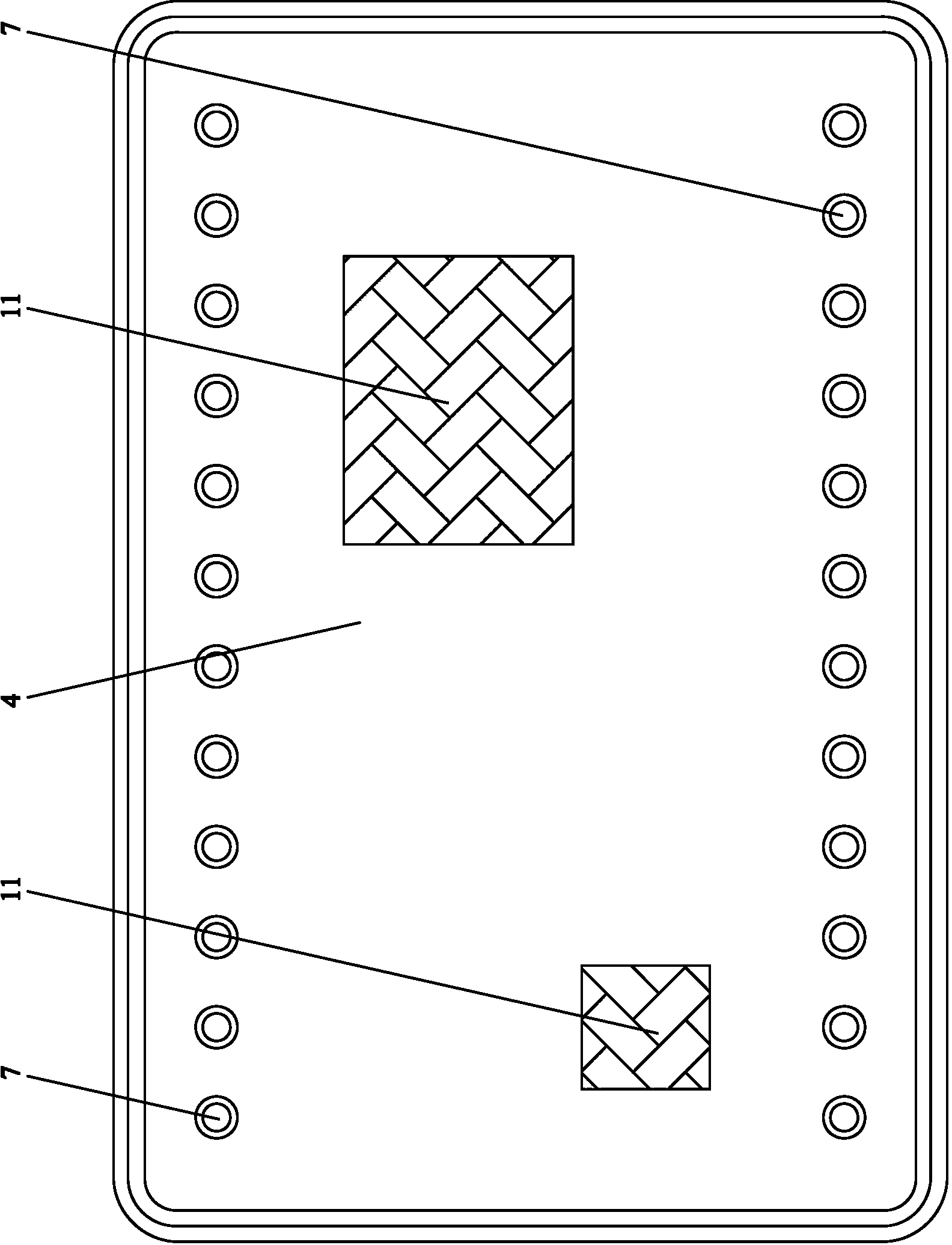
[0034] The metal casing 1 includes a casing base 4 and a casing cover 5, wherein the casing base 4 is a box-shaped structure with an upward opening, and the casing cover 5 covers the opening, so that the casing base 4 A complete metal casing 1 is formed with the casing cover plate 5 and an inner cavity 6 is formed, and the substrate...


PUM


Abstract

The invention relates to an integrated circuit packaging structure which comprises a metal pipe shell and a substrate, wherein the two faces of the substrate are respectively provided with a surface-mounted component and a naked chip. The substrate leads out pins connected through tin soldering, wherein each pin is sleeved with a supporting ring for supporting the substrate from a lower portion. Positions, corresponding to the surface-mounted components or heating components in the naked chips, on the upper inner surface and the lower inner surface of the metal pipe shell are provided with radiating structures. Each radiating structure comprises a heat conductive boss arranged on the inner surface of the metal pipe shell in a protruding mode and corresponds to one corresponding heating component and a radiating pad, wherein one face of each radiating pad is in contact with one corresponding heat conductive boss, and the other face of each radiating pad is in contact with the top of one corresponding heating component. The metal pipe shell comprises a pipe shell base and a pipe shell cover plate, wherein the pipe shell base and the pipe shell plate are packaged in an airtight mode through parallel seam welding or laser welding. According to the integrated circuit packaging structure, packaging of the substrate with double-face layout can be achieved, the integration degree of an integrated circuit can be improved, good radiating can be achieved through the heating components on the double faces of the substrate, reliability of the circuit is guaranteed, an impact-proof function is achieved, and the processing process is simple.

Description

technical field [0001] The invention relates to a package structure and a package method of an integrated circuit, in particular to a package structure and a package method with excellent heat dissipation performance. Background technique [0002] The well-known thick-film assembly metal shell structure packaging technology is generally to assemble surface-mounted devices or bare chips on the front of the substrate; only wire or distribute film-like devices on the back of the substrate, so that the entire back is flat; The way of bonding realizes the connection with the tube shell, and finally the tube shell and the cover sheet are seam-welded to realize the fully airtight packaging structure of the metal tube shell. The disadvantage of this packaging structure is that it is a conventional hermetic packaging design with a relatively low integration level, and the heat-generating device cannot establish a heat dissipation channel with the shell, and the heat cannot be directl...

Claims


Application Information

Patent Timeline
Patent Type & Authority Applications(China)
IPC IPC(8): H01L23/31H01L23/367H01L21/56
Inventor 聂月萍吴猛李杰刘海亮
Owner EAST CHINA INST OF OPTOELECTRONICS INTEGRATEDDEVICE
Why Eureka
Try Eureka