

Method for observing TSV (through-silicon-via) copper crystalline grains
A grain and observation technology, which is applied in the field of microelectronics, can solve the problems of difficult control of the reaction time and speed between the corrosion solution and the metal, damage to the sample surface, poor observation effect, etc., and achieve a strictly controllable and highly repeatable etching process sexual effect
- Summary
- Abstract
- Description
- Claims
- Application Information
AI Technical Summary
Problems solved by technology
Method used
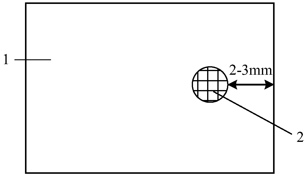
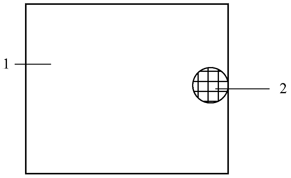
Image

Examples
Embodiment Construction
[0031] In order to make the object, technical solution and advantages of the present invention clearer, various embodiments of the present invention will be described in detail below in conjunction with the accompanying drawings. However, those of ordinary skill in the art can understand that, in each implementation manner of the present invention, many technical details are provided for readers to better understand the present application. However, even without these technical details and various changes and modifications based on the following implementation modes, the technical solution claimed in each claim of the present application can be realized.
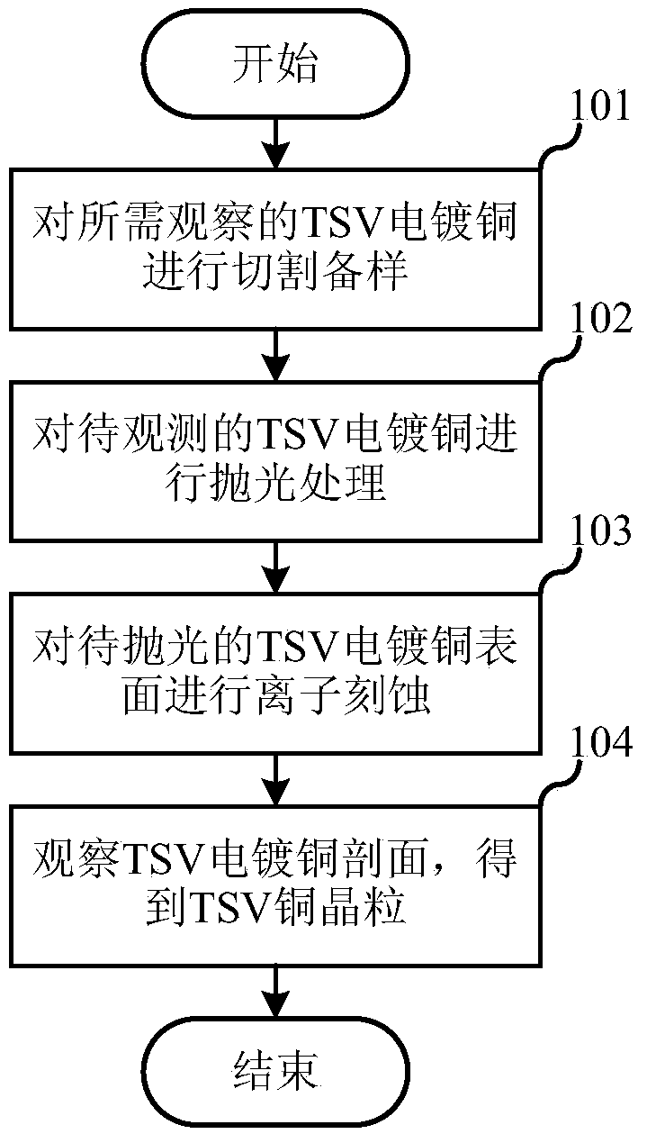
[0032] The first embodiment of the present invention relates to a method for observing TSV copper grains, the specific process is as follows figure 1 shown.
[0033] In step 101, the TSV electroplated copper to be observed is cut and prepared. Specifically, the TSV electroplated copper to be observed is cut with a slow-spe...
PUM
 Abstract
Description
Claims
Application Information