Method for homoepitaxial carbon silicon double atomic layer thin film on sic substrate

A carbon-silicon diatomic, homoepitaxial technology, applied in chemical instruments and methods, from chemically reactive gases, single crystal growth, etc., can solve problems such as the impact of SiC device performance, increase film growth area, and shorten epitaxy time. Effect

Active Publication Date: 2016-10-05
宁波合盛新材料有限公司
View PDF1 Cites 0 Cited by
  • Summary
  • Abstract
  • Description
  • Claims
  • Application Information

AI Technical Summary

Problems solved by technology

[0003] However, there are various defects in SiC that have a serious impact on device performance.

Method used


Image

  • Method for homoepitaxial carbon silicon double atomic layer thin film on sic substrate
  • Method for homoepitaxial carbon silicon double atomic layer thin film on sic substrate
  • Method for homoepitaxial carbon silicon double atomic layer thin film on sic substrate

Examples


Embodiment Construction

[0021] The technical solutions of the present invention will be described in further detail below with reference to the accompanying drawings and embodiments.

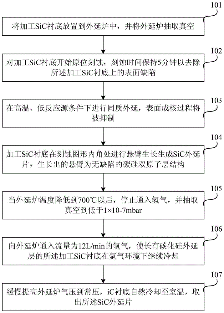
[0022] figure 1 It is a flow chart of Embodiment 1 of the method for homoepitaxial carbon-silicon double atomic layer thin film on SiC substrate of the present invention; as shown in the figure, this embodiment specifically includes:

[0023] Step 101, placing the processed SiC substrate processed by using the original SiC substrate with positive axis 4H or 6H into the epitaxial furnace, and vacuuming the epitaxial furnace;

[0024] Step 102, when the vacuum degree of the epitaxial furnace is lower than 6×10 -7 Inject hydrogen at mbar to keep the pressure at 100mbar and heat the epitaxial furnace. When the temperature reaches 1600 degrees, the hydrogen starts to etch the processed SiC substrate in situ. The etching time is kept for 5 minutes to remove the surface defects on the processed SiC substrate. ;

[0025] St...


PUM

PropertyMeasurementUnit
angleaaaaaaaaaa

Abstract

The invention relates to a SiC substrate homoepitaxy carbon silicon double-atomic-layer film method. The method is characterized by comprising the steps of placing a processed SiC substrate into an epitaxy furnace, vacuumizing the epitaxy furnace, filling hydrogen into the epitaxy furnace to keep the pressure as 100mbar, heating the epitaxy furnace, carrying out in-site etching on the processed SiC substrate, keeping the temperature at 1600 DEG C, filling SiH4 into the epitaxy furnace at the speed of 3ml / min and C3H8 into the epitaxy furnace at the speed of 1.1ml / min, filling carrier hydrogen into the epitaxy furnace at the speed of 4500ml / min, and carrying out cantilever growth at the inner corner position of an etched pattern of the SiC substrate to generate a SiC epitaxial wafer. A grown cantilever is of a non-defective carbon silicon double-atomic-layer structure. According to the SiC substrate homoepitaxy carbon silicon double-atomic-layer film method, a layer of thin complete non-defective cantilever is formed in an etching tabletop of the top end of the positive-axis silicon carbide substrate in an extending mode. Furthermore, epitaxy time is effectively shortened, and the film growth area is improved.

Description

technical field [0001] The invention relates to the technical field of semiconductor materials, in particular to a method for homoepitaxial carbon-silicon double atomic layer thin film on a silicon carbide SiC substrate. Background technique [0002] As one of the representatives of wide band gap semiconductor materials, silicon carbide SiC has superior properties such as large band gap, high breakdown electric field, high thermal conductivity, high electron saturation drift velocity, strong radiation resistance and good chemical stability. It has become a key semiconductor material for the manufacture of a new generation of microelectronic devices and circuits after germanium, silicon, and gallium arsenide. Compared with Si-based devices under the same conditions, SiC-based devices can withstand much higher voltage and microwave power. For example, the ft of SiC MESFET can reach 12-15GHz. [0003] However, there are various defects in SiC that seriously affect the device p...

Claims


Application Information

Patent Timeline
Patent Type & Authority Patents(China)
IPC IPC(8): H01L21/20C30B25/02
CPCC30B25/186C30B25/20C30B25/205C30B29/36H01L21/02378H01L21/02529H01L21/02634H01L21/02661
Inventor 贾仁需辛斌宋庆文张艺蒙闫宏丽
Owner 宁波合盛新材料有限公司
Why Eureka
Try Eureka