Method for temporarily bonding and debonding slice applied to semiconductor manufacturing process

A temporary bonding and semiconductor technology, applied in semiconductor/solid-state device manufacturing, electrical components, circuits, etc., can solve the problems of high temperature and environment requirements, silicon wafer pollution in process steps, high process complexity, etc., and achieve low requirements, The effect of strong operation and practicability and simple process

Active Publication Date: 2014-01-01
中国东方电气集团有限公司
View PDF3 Cites 5 Cited by
  • Summary
  • Abstract
  • Description
  • Claims
  • Application Information

AI Technical Summary

Problems solved by technology

[0004] The above-mentioned patents are the same as the prior art, the adhesives used are special materials purchased from foreign or domestic specialized manufacturers, the cost is very high, and this adhesive will cause pollution to the silicon wafer, the device itself and the operator , because the existing adhesives are all non-degradable organic materials, so on the one hand, there will be unavoidable pollution on the bonded silicon wafers, which can be controlled to a small extent, but still exists. In the bonding process of the existing technology, some need to perform pretreatment processes such as slotting or engraving on the silicon wafer before bonding, and some need to use spin coating or spraying during bonding. Some methods need to be bonded in a high-temperature and high-pressure environment, and some need to be baked and heated to fix the sheet and the mother chip after bonding, and the temperature and environment requirements are also higher during the debonding process. The complexity is very high, and the increased process steps are also likely to introduce more defects and pollution on the surface of the silicon wafer, which may affect the performance of the device

Method used


Image

  • Method for temporarily bonding and debonding slice applied to semiconductor manufacturing process
  • Method for temporarily bonding and debonding slice applied to semiconductor manufacturing process
  • Method for temporarily bonding and debonding slice applied to semiconductor manufacturing process

Examples


Embodiment 1

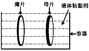
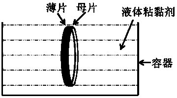
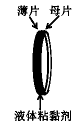
[0023] A method for temporary bonding and debonding of wafers used in semiconductor manufacturing process Step 1: Place semiconductor wafers and mother wafers to be bonded into a container filled with liquid adhesive. The depth of the liquid in the container needs to be greater than that of the wafer and mother wafer The diameter of the sheet, the semiconductor flakes are single crystals, polycrystals and non-wafers of group IV materials and III-V materials; the semiconductor mother sheet is a single crystal of the same material with the same size and shape as the semiconductor sheet, Polycrystalline and non-wafer; the thickness of the sheet is 50 μm to 200 μm; the thickness of the mother sheet is 150 μm to 1000 μm; Step 2: In a container containing a liquid adhesive, place the sheet and the mother sheet in parallel Gradually approach and contact alignment, so that the two are sticky and adsorbed together, and the edges of the two are aligned. When the sheet and the mother shee...

Embodiment 2

[0025]A method for temporary bonding and debonding of sheets used in semiconductor manufacturing processes, step 1: placing semiconductor sheets and mother sheets to be bonded in a container filled with a liquid adhesive, the liquid adhesive being deionized water or ethanol. The container holding the liquid adhesive is a liquid pool or a liquid tank. The depth of the liquid in the container needs to be greater than the diameter of the sheet and the mother sheet. The semiconductor sheet is a single crystal, polycrystalline and Non-wafer, group IV materials such as Ge, group III-V materials such as InP, etc.; the semiconductor mother sheet is single crystal, polycrystal and non-wafer of the same material with the same size and shape as the semiconductor sheet; the thickness of the sheet 200 μm; the thickness of the mother sheet is 1000 μm; Step 2: In a container containing a liquid adhesive, gradually move the thin sheet and the mother sheet closer together in a parallel manner ...

Embodiment 3

[0027] A method for temporary bonding and debonding of sheets used in semiconductor manufacturing processes, step 1: placing semiconductor sheets and mother sheets to be bonded in a container filled with a liquid adhesive, the liquid adhesive being deionized water or ethanol. The container holding the liquid adhesive is a liquid pool or a liquid tank. The depth of the liquid in the container needs to be greater than the diameter of the sheet and the mother sheet. The semiconductor sheet is a single crystal, polycrystalline and Non-wafer, group IV materials such as Si, group III-V materials such as GaAs; the semiconductor mother sheet is single crystal, polycrystal and non-wafer of the same material with the same size and shape as the semiconductor sheet; the thickness of the sheet is 50 μm; the thickness of the mother sheet is 150 μm; step 2: in a container containing a liquid adhesive, gradually move the thin sheet and the mother sheet closer together in a parallel manner and...


PUM


Abstract

The invention belongs to semiconductor integrated circuit manufacturing processes, and particularly relates to a method for bonding and debonding a slice applied to a semiconductor manufacturing process. The semiconductor slice and a semiconductor master slice to be bonded are placed in a contained filled with liquid sticky agents, the depth of the liquid in the container needs to be larger than the diameter of the slice and the master slice, and the semiconductor slice is a single-crystal wafer or a multi-crystal wafer or an amorphous wafer made of IV-group materials and III-V-group materials. The semiconductor master slice is a single-crystal wafer or a multi-crystal wafer or an amorphous wafer with the size, the shape and the materials identical to those of the semiconductor slice. Compared with the prior art, the method is lower in material cost, enables materials to be obtained more easily, is stronger in protection on the slice and operators, more easier in technological process, lower in requirement for equipment and higher in operability and practicality, and has the creative and technical advantages. The liquid sticky agents are adopted as the materials of the slice bonding technology, and deionized water or ethyl alcohol is used as the materials in specific examples.

Description

technical field [0001] The invention belongs to the manufacturing process of semiconductor integrated circuits, in particular to a method for temporary bonding and debonding of thin slices used in the semiconductor manufacturing process. Background technique [0002] In order to meet the technical development and market demands of high performance and low energy consumption, industries such as microelectronics, optoelectronics, and power devices based on semiconductor wafers need to continuously pursue the development of miniaturization and thinning of devices. Taking the power device insulated gate bipolar transistor (IGBT) as an example, the first generation of IGBT products born in the 1980s had a device thickness of more than 500 μm. After two decades of rapid development, the mainstream fifth-generation IGBT on the market today The device thickness of the sixth-generation IGBT products has been reduced to 100 μm or even smaller, and correspondingly, the energy loss of t...

Claims


Application Information

Patent Timeline
Patent Type & Authority Applications(China)
IPC IPC(8): H01L21/683
CPCH01L21/2007
Inventor 王思亮胡强张世勇樱井建弥
Owner 中国东方电气集团有限公司
Why Eureka
Try Eureka