A packaging structure and packaging method for radio frequency inductors

A packaging structure and packaging method technology, applied in the direction of circuits, electrical components, electrical solid devices, etc., can solve the problems of unfavorable market promotion of portable devices, process difficulty and high production cost, and affect Q value, so as to overcome process difficulty and process The effect of reducing cost and production cost and improving Q value

Active Publication Date: 2016-01-27
JIANGYIN CHANGDIAN ADVANCED PACKAGING CO LTD
View PDF4 Cites 0 Cited by
  • Summary
  • Abstract
  • Description
  • Claims
  • Application Information

AI Technical Summary

Problems solved by technology

[0003] At present, silicon-based inductors or low-temperature ceramic inductors realized by semiconductor rewiring technology in portable devices have the characteristics of good high-frequency performance, high precision, high stability, and large size, but their process difficulty and production cost are relatively high; The existence of eddy current loss in the inductor matrix at high frequencies affects the Q value; its size is also limited by the presence of substrates (such as silicon substrates, ceramic substrates) and further reduction, which is not conducive to the market promotion of portable devices

Method used


Image

  • A packaging structure and packaging method for radio frequency inductors
  • A packaging structure and packaging method for radio frequency inductors
  • A packaging structure and packaging method for radio frequency inductors

Examples


Embodiment Construction

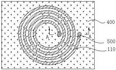
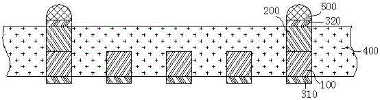
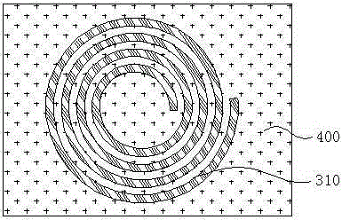
[0047] see Figure 1 to Figure 3 , is an embodiment of a packaging structure of a radio frequency inductor of the present invention, which is formed by a semiconductor packaging process. The inductance coil 110 is in a spiral shape and is formed by continuous metal wires 100 with a certain thickness and a certain gap. Metal pillars 200 vertically connected to the metal wire 100 are provided at the inner and outer ports of the metal wire 100, and the metal pillars 200 are perpendicular to the plane where the inductance coil 110 is located. The cross-section of the metal pillars 200 is circular, rectangular or polygonal. The width of the metal post 200 is not greater than the width of the metal line 100 . The gaps between the adjacent metal wires 100 and the periphery of the metal wires 100 and the metal pillars 200 are sealed with a plastic sealing material, and the plastic sealing material is a thermosetting resin. The lower surface of the metal wire 100 and the upper end su...


PUM


Abstract

The invention relates to a packaging structure of a radio frequency inductor and a packaging method thereof, belonging to the technical field of semiconductor packaging. The process: provide a metal carrier (T100); set a photoresist layer I (T210) on the metal carrier (T100), and use an electroplating process to form a metal line in the photoresist layer I opening pattern (T211) ( 100); using the same process, set metal posts (200) at the inner and outer ports of the inductance coil (110); remove the photoresist plastic-encapsulated metal wires (100) and metal posts (200); remove the metal carrier (T100), and place The exposed surfaces of the metal wire (100) and the metal post (200) are respectively coated with a metal coil protection layer (310) and a metal post protection layer (320); solder balls (500) are arranged on the metal post protection layer (320) to realize inductance connection to the carrier board. The radio frequency inductor of the present invention has no silicon or ceramics as a substrate, can reduce process difficulty and production cost, improve Q value, and reduce inductance size, so as to facilitate market promotion of portable devices.

Description

technical field [0001] The invention relates to a packaging structure of a radio frequency inductor and a packaging method thereof, belonging to the technical field of semiconductor packaging. Background technique [0002] Due to the continuous improvement of IC (integrated circuit) design and process technology, the scale of integrated circuits is getting larger, the complexity and integration are getting higher and higher, and the entire system, including analog circuit parts and digital circuit parts, can be integrated into one chip. . Since inductors are used in all important subunits of radio frequency integrated circuits, inductors occupy a large area of ​​radio frequency integrated circuits, and their performance directly affects the overall performance of radio frequency integrated circuits. Therefore, radio frequency inductors are used to achieve low An important component of low cost, low voltage, low power RFIC (Radio Frequency Integrated Circuit). [0003] At p...

Claims


Application Information

Patent Timeline
Patent Type & Authority Patents(China)
IPC IPC(8): H01L23/64H01L21/02
CPCH01L2924/0002
Inventor 卞新海郭洪岩张黎陈锦辉赖志明
Owner JIANGYIN CHANGDIAN ADVANCED PACKAGING CO LTD
Why Eureka
Try Eureka