
OLED (Organic Light Emitting Diode) pixel structure and OLED display device

A technology of pixel structure and thin film transistor, applied in the direction of organic semiconductor devices, semiconductor devices, electrical components, etc., can solve the problems that the display screen cannot be effectively used and the utilization rate of the display panel is low, so as to improve the utilization rate of the light source and the utilization rate. , the effect of reducing the area

Inactive Publication Date: 2014-01-08
BOE TECH GRP CO LTD
View PDF4 Cites 22 Cited by
  • Summary
  • Abstract
  • Description
  • Claims
  • Application Information

AI Technical Summary

Problems solved by technology

Since the area corresponding to the blank window is only used as a transmission area and cannot be effectively used for displaying images, the utilization rate of the display panel is low

Method used


Image

  • OLED (Organic Light Emitting Diode) pixel structure and OLED display device
  • OLED (Organic Light Emitting Diode) pixel structure and OLED display device
  • OLED (Organic Light Emitting Diode) pixel structure and OLED display device

Examples


Embodiment 1

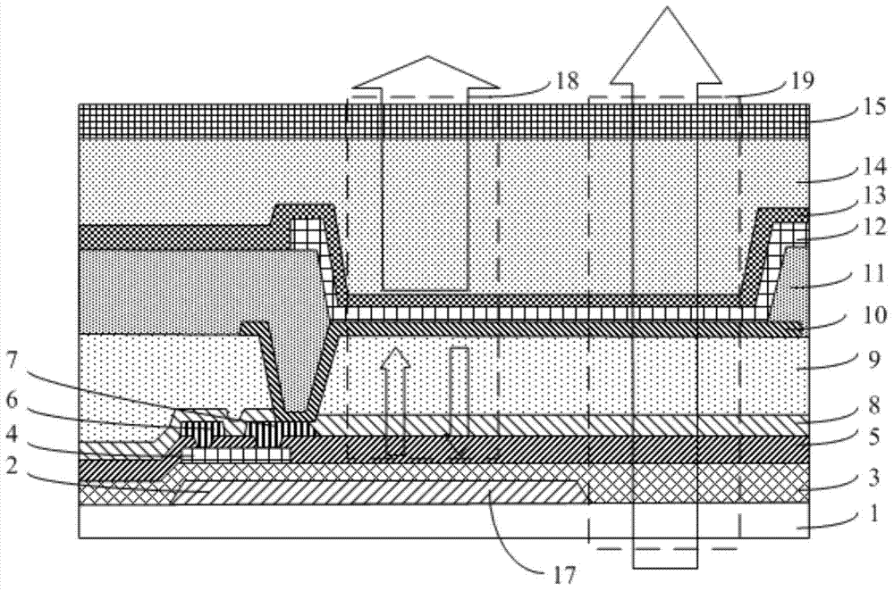
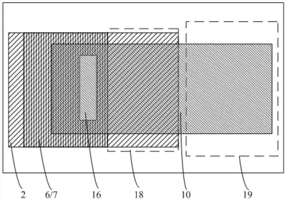
[0025] In this embodiment, in the thin film transistor of the pixel structure, the driving electrode includes a gate, and a source and a drain arranged in the same layer, and the reflective layer is formed by extending the gate to the center of the pixel structure; the reflective layer and the gate use the same material, the thickness of the reflective layer is equal to the thickness of the grid.

[0026] In this embodiment, the OLED device has a top emission structure, that is, the light emitted by the OLED device is emitted from bottom to top. In an OLED device, an anode and a cathode are arranged oppositely, and the anode and the cathode are formed of a transparent electrode material or a metal alloy material having the same transparent effect; the reflective layer is arranged below the anode and partially overlaps with the anode in the direction of orthographic projection.

[0027] Such as figure 1 , 2 As shown, in this embodiment, as an example of a pixel structure that...

Embodiment 2

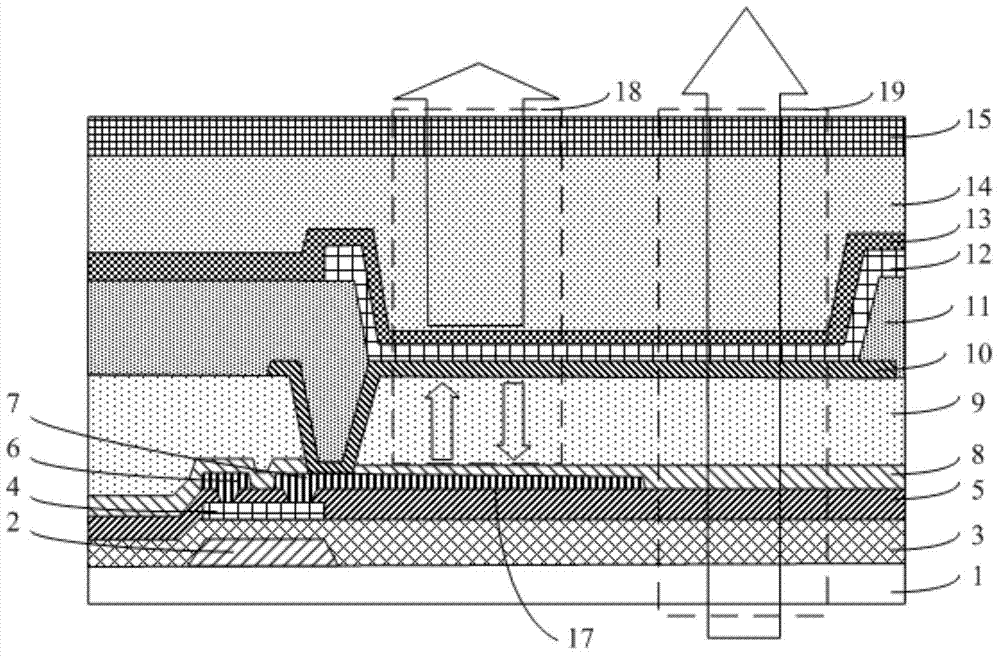
[0039] In this embodiment, in the thin film transistor of the pixel structure, the driving electrode includes a gate, and a source and a drain arranged in the same layer, and the reflective layer is formed by extending the drain toward the center of the pixel structure; the reflective layer and the drain use the same material, the thickness of the reflective layer is equal to the thickness of the drain.

[0040] In this embodiment, the OLED device is still a top-emission type structure, and the opposite anode and cathode are formed of transparent electrode materials or metal alloy materials with the same transparent effect; Partially overlap in the projection direction.

[0041] Such as image 3 As shown, in this embodiment, as an example of a pixel structure that uses a top-gate thin film transistor to drive an OLED device, the thin film transistor includes a gate 2 disposed above a substrate 1, a gate insulating layer 3, an active layer 4, an engraved Etching barrier layer...

Embodiment 3

[0047] The difference between this embodiment and Embodiments 1 and 2 is that in the pixel structure of this embodiment, the thin film transistor is a bottom-gate structure.

[0048] In this embodiment, the active layer of the bottom-gate TFT is relatively disposed below the gate. Similar to Embodiments 1 and 2, in this embodiment, the reflective layer in the pixel structure can still be formed by extending the gate or drain toward the center of the pixel structure. The function of the reflective layer in the pixel structure is the same as that in Embodiment 1 or Embodiment 2, which can also improve the light source utilization rate of the OLED device; the transmissive area can realize transparent display. Compared with the pixel structure in the prior art, this The embodiment forms a reflective area and a transmissive area in the area corresponding to the blank window in the prior art, which reduces the area of ​​the blank window and improves the utilization rate of the displ...


PUM


Abstract

The invention belongs to the technical field of display, and particularly relates to an OLED (Organic Light Emitting Diode) pixel structure and an OLED display device. The OLED pixel structure comprises a TFT (Thin Film Transistor) and an OLED device, wherein a driving electrode is arranged in the TFT, and the driving electrode is used for controlling the OLED device to emit lights; the OLED pixel structure comprises a transmission area and a reflection area, wherein the reflection area is internally provided with a reflection layer formed by stretching the driving electrode. The OLED pixel structure disclosed by the invention has the beneficial effects that the utilization rate of a light source can be effectively increased, and the utilization rate of a display panel can be effectively increased.

Description

technical field [0001] The invention belongs to the field of display technology, and in particular relates to an OLED pixel structure and an OLED display device. Background technique [0002] Transparent display is a hot technology direction in recent years. As the mainstream of existing flat panel display, TFT (Thin Film Transistor, Thin Film Transistor)-LCD (Liquid Crystal Display: Liquid Crystal Display) and AMOLED (Active Matrix Organic Light-Emitting Device, Actively driven electroluminescent devices) can realize transparent display, especially AMOLED transparent display is better, which is also the mainstream research direction. [0003] OLED is a light-emitting device that uses organic solid-state semiconductors as light-emitting materials. It has broad application prospects due to its advantages such as simple preparation process, low cost, low power consumption, high luminous brightness, and wide operating temperature range. Compared with the liquid crystal display...

Claims


Application Information

Patent Timeline
Patent Type & Authority Applications(China)
IPC IPC(8): H01L27/32H01L51/52
CPCH01L29/41733H01L29/42384H01L29/78633H01L27/124H01L29/7869H10K2102/3026H10K59/8051H10K59/878H10K59/80524H10K59/1213H10K10/462H10K50/81H10K50/816H10K50/828H10K50/856H10K59/123H10K59/125H10K59/131H10K2102/351H01L29/78663H01L29/78672
Inventor 石领永山和由史世明
Owner BOE TECH GRP CO LTD
Learn More