Scanning signal line driving circuit, display device provided therewith, and scanning signal line driving method

A technology for scanning signal lines and driving circuits, which is applied to electrical components, information storage, static indicators, etc., and can solve problems such as reduced reliability of transistors and large threshold fluctuations

Active Publication Date: 2014-01-08
SHARP KK
View PDF7 Cites 15 Cited by
  • Summary
  • Abstract
  • Description
  • Claims
  • Application Information

AI Technical Summary

Problems solved by technology

As a result, the threshold fluctuations that occur in these transistors M5 and M6 become larger, thus resulting in reduced reliability of the transistors

Method used


Image

  • Scanning signal line driving circuit, display device provided therewith, and scanning signal line driving method
  • Scanning signal line driving circuit, display device provided therewith, and scanning signal line driving method
  • Scanning signal line driving circuit, display device provided therewith, and scanning signal line driving method

Examples


no. 1 Embodiment approach >

[0137]

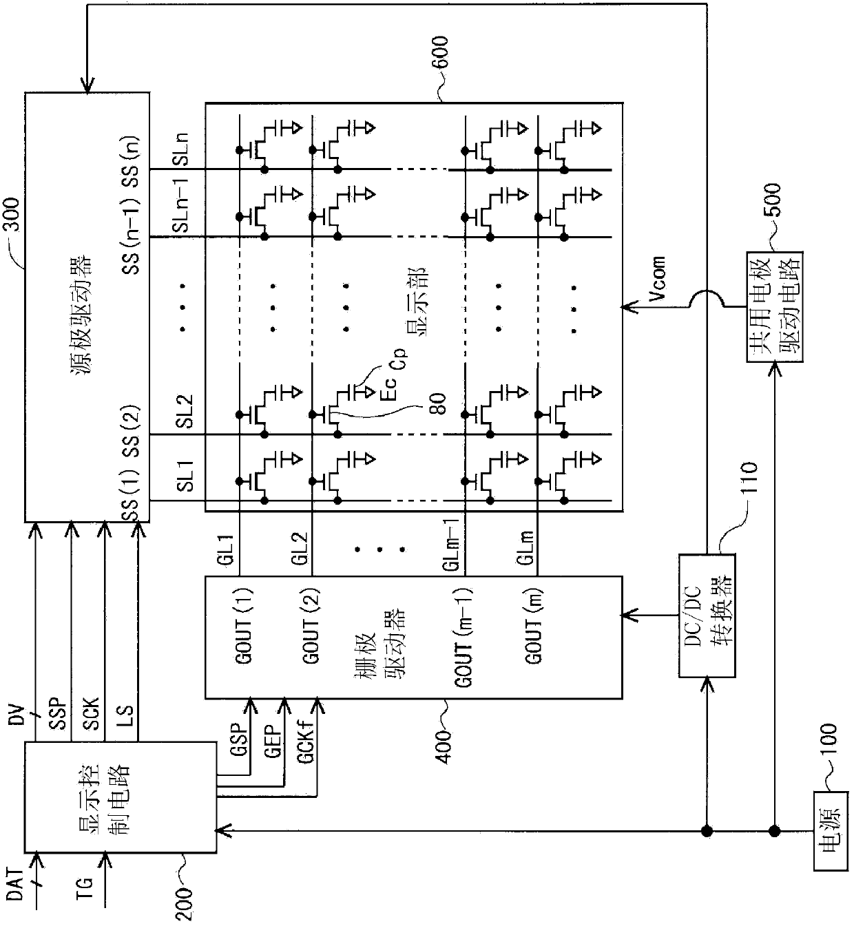
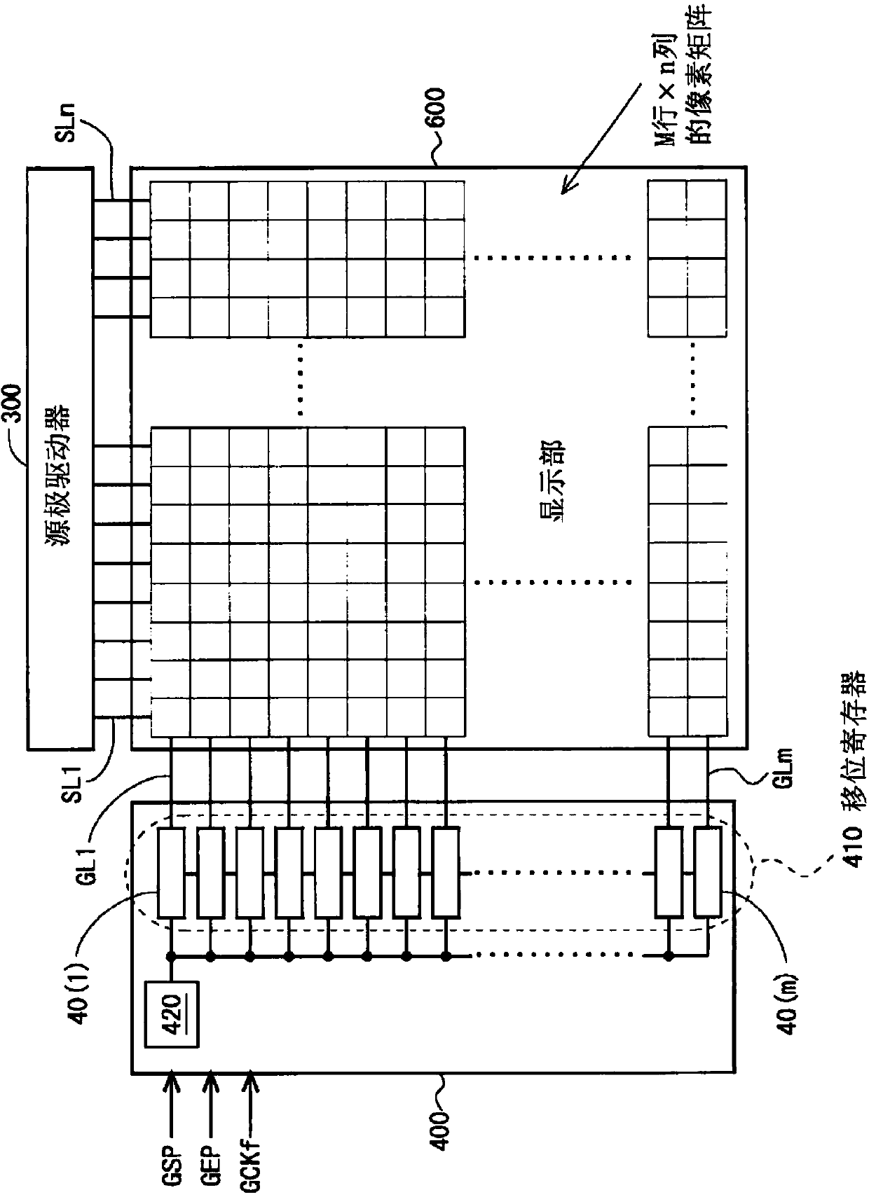
[0138] figure 1 It is a block diagram showing the overall configuration of the active matrix liquid crystal display device according to the first embodiment of the present invention. Such as figure 1 As shown, the liquid crystal display device includes: a power supply 100, a DC / DC converter 110, a display control circuit 200, a source driver (video signal line drive circuit) 300, a gate driver (scanning signal line drive circuit) 400, a common electrode The driving circuit 500 and the display unit 600 . In addition, the gate driver 400 is formed on the display panel including the display portion 600 using amorphous silicon, polycrystalline silicon, microcrystalline silicon, or an oxide semiconductor (such as IGZO). That is, in this embodiment, the gate driver 400 and the display unit 600 are formed on the same substrate (the array substrate which is one of the two substrates constituting the liquid crystal panel). Accordingly, the frame area of ​​the liquid cry...

no. 2 Embodiment approach >

[0209]

[0210] Figure 22 It is a signal waveform diagram for explaining the detailed operation of the gate driver 400 according to the second embodiment of the present invention. In addition, the overall configuration and operation of the liquid crystal display device, the configuration and operation of the gate driver 400, the configuration and operation of the bistable circuit, and the configuration and operation of the clock control circuit 420 are the same as those of the above-mentioned first embodiment. These descriptions are therefore omitted.

[0211] In the above-mentioned first embodiment, a vertical retrace period (about 8.3 msec) of about 1 / 2 the length of one vertical scan period is provided, and the drive frequency in the writing period is doubled the general drive frequency (60 Hz). That is 120Hz (about 8.3msec). In contrast, in this embodiment, if Figure 22 As shown, set a vertical retrace period (approximately 11.1msec) of approximately 2 / 3 the length ...

no. 3 Embodiment approach >

[0215]

[0216] Figure 23 It is a signal waveform diagram for explaining the detailed operation of the gate driver 400 according to the third embodiment of the present invention. In addition, the overall configuration and operation of the liquid crystal display device, the configuration and operation of the gate driver 400, the configuration and operation of the bistable circuit, and the configuration and operation of the clock control circuit 420 are the same as those of the above-mentioned first embodiment. These descriptions are therefore omitted.

[0217] In the above-mentioned first embodiment, a vertical retrace period (about 8.3 msec) of about 1 / 2 the length of one vertical scan period is provided, and the drive frequency in the writing period is doubled the general drive frequency (60 Hz). That is 120Hz (about 8.3msec). In addition, in the above-mentioned second embodiment, the vertical retrace period (about 11.1 msec) having a length of approximately 2 / 3 of one v...


PUM


Abstract

The purpose of this invention is to provide a scanning signal line driving circuit with increased reliability of switching elements while reducing power consumption. In the vertical blanking interval, an end signal (ED) changes from the low level to the high level. The potential of the 1st through (m-1)st stage first nodes (N1) of cascade-connected m-stage bistable circuits contained in a shift register of the scanning signal line driving circuit is reliably maintained at the low level, and the potential of 1st through (m-1)st stage second nodes (N2) changes from the high level to the low level. In the mth stage bistable circuit, the potential of the mth stage first node (N1) changes from the high level to the low level, and the potential of the mth stage second node (N2) is maintained at the low level. Further, supply of the clock signal (CKA, CKB) to the bistable circuit is stopped. Until the write period in the subsequent vertical scanning period, the potential of the first nodes (N1) and the potential of the second nodes (N2) in each stage is maintained at the low level.

Description

technical field [0001] The present invention relates to a scanning signal line driving circuit, a display device equipped with it, and a method for driving a scanning signal line, and in particular to a scanning signal line driving circuit suitable for singulation, a display device equipped with it, and a display device equipped with the scanning signal line driving circuit. The driving method of the scanning signal line. Background technique [0002] Conventionally, a gate driver (scanning signal line drive circuit) for driving gate lines (scanning signal lines) of a liquid crystal display device is often mounted as an IC (Integrated Circuit) chip on the periphery of a substrate constituting a liquid crystal panel. However, in recent years, there have been increasing cases where gate drivers are directly formed on substrates. Such a gate driver is called a "monolithic gate driver" and so on. [0003] In a liquid crystal display device including a monolithic gate driver, a...

Claims


Application Information

Patent Timeline
Patent Type & Authority Applications(China)
IPC IPC(8): G09G3/36G02F1/133G09G3/20
CPCG09G3/3677G09G2310/0286G11C19/28G02F1/133G09G3/20G09G3/36G09G3/3696H03K3/012
Inventor 岩濑泰章
Owner SHARP KK
Why Eureka
Try Eureka