Plasma reaction chamber and plasma device with same
A plasma and reaction chamber technology, used in semiconductor/solid-state device manufacturing, discharge tubes, electrical components, etc., can solve the problems of reducing equipment yield, increasing use costs, breaking vacuum, etc., to improve etching efficiency, prolong Service life, effect of reducing heating time
- Summary
- Abstract
- Description
- Claims
- Application Information
AI Technical Summary
Problems solved by technology
Method used
Image

Examples
Embodiment Construction
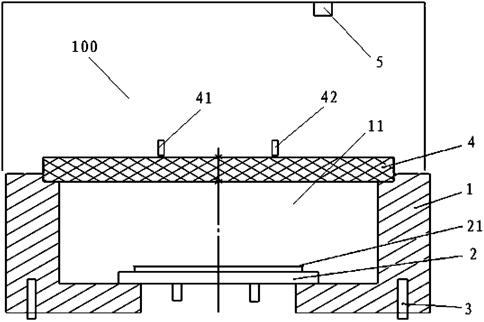
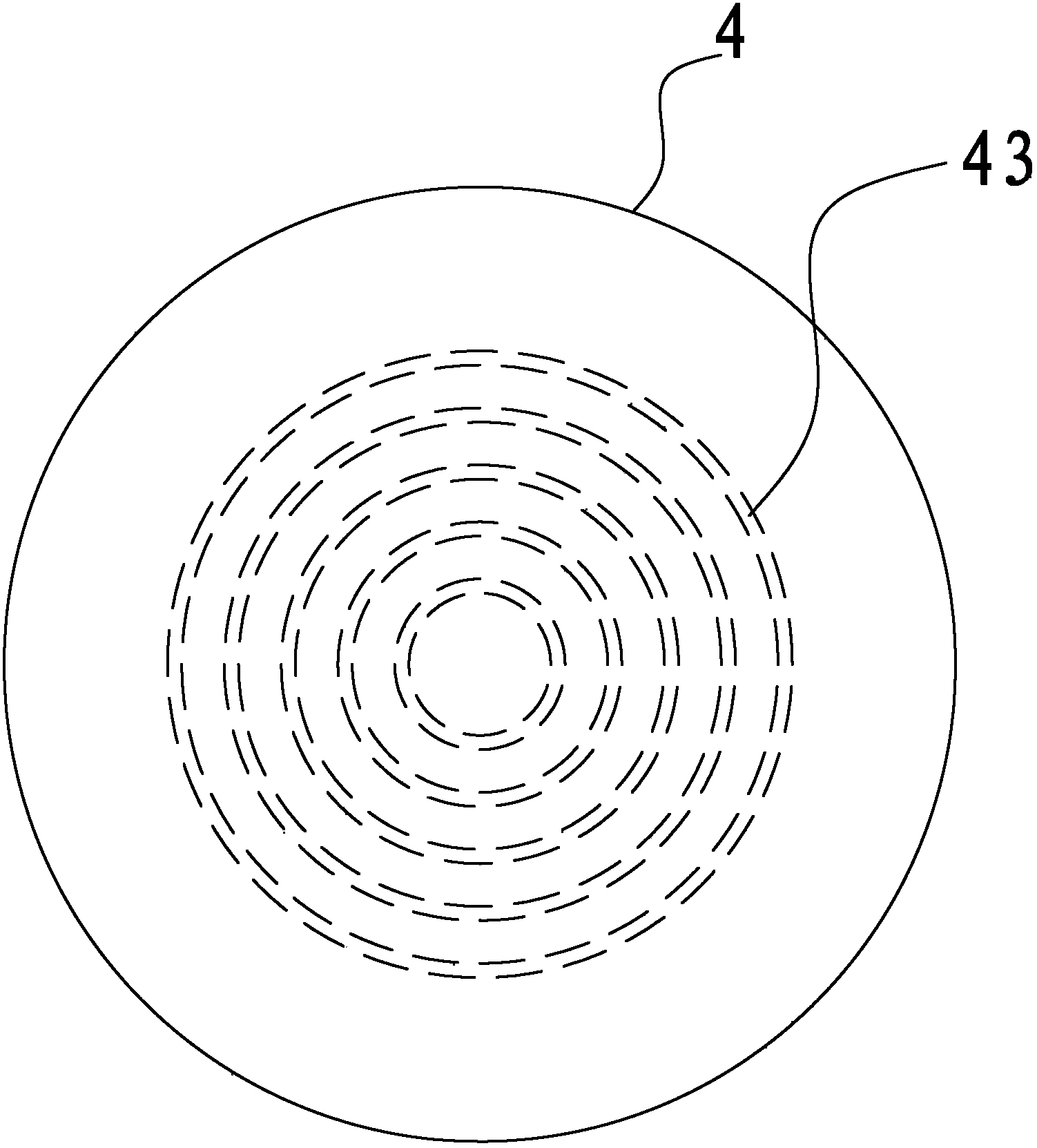
[0025] Embodiments of the present invention are described in detail below, examples of which are shown in the drawings, wherein the same or similar reference numerals designate the same or similar elements or elements having the same or similar functions throughout. The embodiments described below by referring to the figures are exemplary and are intended to explain the present invention and should not be construed as limiting the present invention.
[0026] In describing the present invention, it should be understood that the terms "center", "longitudinal", "transverse", "length", "width", "thickness", "upper", "lower", "front", " The orientations or positional relationships indicated by "rear", "left", "right", "vertical", "horizontal", "top", "bottom", "inner", "clockwise", "counterclockwise" are based on the attached The orientation or positional relationship shown in the figure is only for the convenience of describing the present invention and simplifying the description...
PUM
 Abstract
Description
Claims
Application Information
 - Generate Ideas
- Intellectual Property
- Life Sciences
- Materials
- Tech Scout
- Unparalleled Data Quality
- Higher Quality Content
- 60% Fewer Hallucinations
Browse by: Latest US Patents, China's latest patents, Technical Efficacy Thesaurus, Application Domain, Technology Topic, Popular Technical Reports.
© 2025 PatSnap. All rights reserved.Legal|Privacy policy|Modern Slavery Act Transparency Statement|Sitemap|About US| Contact US: help@patsnap.com