Semiconductor device and system using same

A technology of semiconductors and devices, applied in the field of semiconductor devices, can solve the problems of increasing the cost of the driving circuit design change system, etc.

Active Publication Date: 2014-01-15
RENESAS ELECTRONICS CORP
View PDF11 Cites 13 Cited by
  • Summary
  • Abstract
  • Description
  • Claims
  • Application Information

AI Technical Summary

Problems solved by technology

In this way, although the JFET has excellent long-term reliability and is easy to manufacture, since the driving voltage of the gate is greatly different from that of a general MOSFET, a large design change of the driving circuit is required, and the problem of increasing the cost of the entire system arises.

Method used


Image

  • Semiconductor device and system using same
  • Semiconductor device and system using same
  • Semiconductor device and system using same

Examples


Embodiment approach )

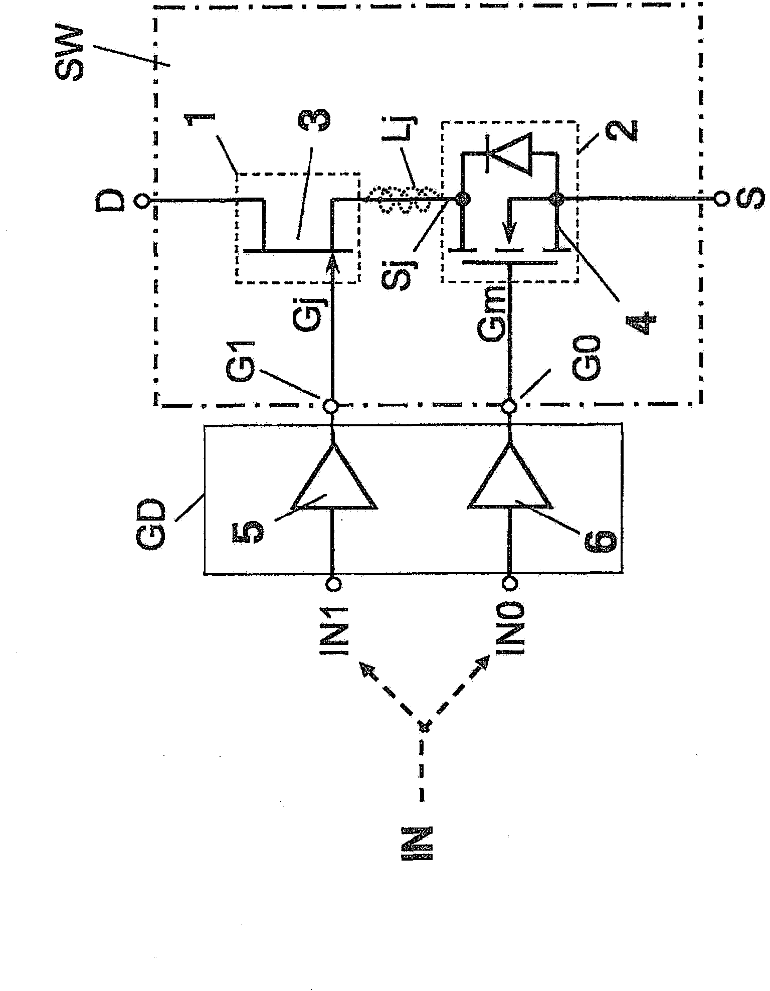
[0054] 1. Switch circuit

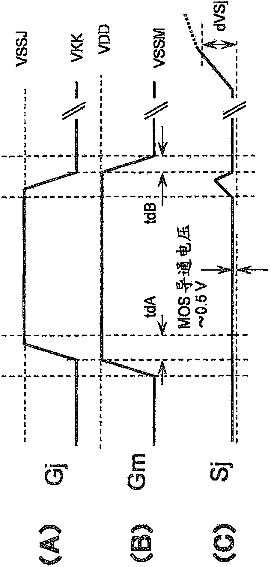
[0055] picture figure 1 As shown, the semiconductor integrated circuit device SW includes two semiconductor chips 1 , 2 . A normally-on SiC JFET 3 is formed in the semiconductor chip 1 , and a normally-off Si-type MOSFET 4 is formed in the semiconductor chip 2 . A SiC JFET 3 and a Si type MOSFET 4 are connected in cascade between a terminal D and a terminal S provided in the semiconductor device SW. That is, between the terminal S and the terminal D, the source-to-drain path of the SiC JFET 3 and the source-to-drain path of the Si-type MOSFET 4 are connected in series. A signal from the drive circuit GD is supplied to the semiconductor device SW. In the drive circuit GD, the gate drive circuits 5 and 6 receive the signals IN1 and IN0 that change according to the input signal IN, and supply the signals that change according to the input signal IN to terminals G1 and G0 of the semiconductor device SW. The terminal G1 is connected to the gate Gj, a...


PUM


Abstract

The invention provides a semiconductor device and a system using the same. The semiconductor device is configured with a normally-on SiCJFET and a normally-off Si-type MOSFET. The normally-on SiCJFET and the normally-off Si-type MOSFET are coupled in cascade and configure a switching circuit. According to one input signal, the normally-on SiCJFET and the normally-off Si-type MOSFET are controlled so as to have a period in which both transistors are set in an OFF state. According to the invention, the semiconductor device configured with the normally-on JFET and the normally-off MOSFET which are coupled in cascade can be prevented from breakdown due to mis-conduction and the like.

Description

[0001] (Cross-reference to related application) [0002] The disclosure of Japanese Patent Application No. 2012-136591 filed on Jun. 18, 2012, including specification, drawings and abstract, is hereby incorporated by reference in its entirety. technical field [0003] The present invention relates to a semiconductor device and a technique applicable to, for example, a power semiconductor device and a system using the semiconductor device. Background technique [0004] Under the large social movement of protecting the global environment, the importance of the electronic industry to reduce the burden on the environment has increased. In particular, power semiconductor devices (hereinafter also referred to as power devices) are used in inverter devices for trains, hybrid vehicles, and electric vehicles, inverter devices for air conditioners, power supply systems for consumer devices such as personal computers, and the like. The performance improvement of power devices has grea...

Claims


Application Information

Patent Timeline
Patent Type & Authority Applications(China)
IPC IPC(8): H03K17/567H03K17/687
CPCH03K17/102H03K17/107H03K17/567H03K2017/6875H01L29/7827H01L23/49562H01L23/49575H01L2224/0603H01L2224/48091H01L2224/48247H01L2224/49111H01L2924/30107H01L2924/3011H01L2924/13091H01L2924/13062H01L29/1608H01L2924/00014H01L2924/00H01L27/0883H03K3/012H01L27/098H02P27/06
Inventor 金泽孝光秋山悟
Owner RENESAS ELECTRONICS CORP
Why Eureka
Try Eureka