
PCB for on-board integration of LED

A positive electrode and negative electrode technology, which is applied in the PCB field, can solve the problems of the positive electrode and the negative electrode being easily oxidized by heat, the LED service life is not long, and the luminous effect is not good, so as to improve the LED luminous effect, not easy to oxidize, and improve the light source. small high effect

Inactive Publication Date: 2014-01-15
杨睿涵
View PDF0 Cites 1 Cited by
  • Summary
  • Abstract
  • Description
  • Claims
  • Application Information

AI Technical Summary

Problems solved by technology

At present, in the PCB of the LED lamp body, there are usually only gold-plated or silver-plated layers on the positive lead and negative lead. Although the silver-plated layer improves the luminous effect, the positive and negative electrodes on the PCB are easily oxidized by heat, resulting in a short service life of the LED

Method used


Image

  • PCB for on-board integration of LED

Examples


Embodiment Construction

[0012] The present invention will be further explained below in conjunction with the accompanying drawings and specific embodiments. It should be understood that the following specific embodiments are only used to illustrate the present invention and are not intended to limit the scope of the present invention. It should be noted that the words "front", "rear", "left", "right", "upper" and "lower" used in the following description refer to the directions in the drawings, and the words "inner" and "outer ” refer to directions towards or away from the geometric center of a particular part, respectively.

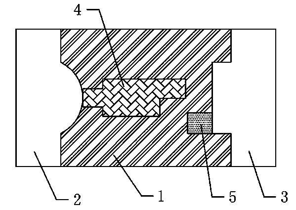
[0013] like figure 1 As shown, a PCB for integration on an LED board disclosed by the present invention includes a PCB1, a positive electrode sheet 2 and a negative electrode sheet 3, and the positive electrode sheet 2 and the negative electrode sheet 3 are respectively arranged at both ends of the PCB1, and the described The positive electrode sheet 2 is provided with a posit...


PUM


Abstract

The invention discloses a PCB for on-board integration of an LED. The PCB for on-board integration of the LED comprises the PCB, a positive plate and a negative plate, wherein the positive plate and the negative plate are arranged at the two ends of the PCB respectively; a positive electrode lead sheet is arranged on the positive plate and extends to the middle of the PCB; a negative electrode lead sheet is arranged on the negative plate and also extends to the middle of the PCB; the positive electrode lead sheet and the negative electrode lead sheet are respectively provided with a silver coating; the positive plate and the negative plate are respectively provided with gold plating. Compared with the traditional mode that electrodes and pole pieces of the PCB are provided with simplex plating, the PCB for on-board integration of the LED improves the light source effect of an LED lamp body, the stability of the PCB is enhanced, and the overall service life of the LED is prolonged.

Description

[0001] technical field [0002] The invention relates to a PCB, in particular to a PCB for integration on an LED board. Background technique [0003] PCB (Printed Circuit Board), also known as printed circuit board, printed circuit board, is an important electronic component, a support for electronic components, and a provider of electrical connections for electronic components. Because it is made using electronic printing, it is called a "printed" circuit board. Before the appearance of printed circuit boards, the interconnection between electronic components was achieved by direct connection of wires, but now, printed circuit boards have occupied an absolute dominant position in the electronics industry. According to the number of circuit layers, PCB is divided into single-sided board, double-sided board and multi-layer board. Common multi-layer boards are generally 4-layer boards or 6-layer boards, and complex multi-layer boards can reach dozens of layers. Single-S...

Claims


Application Information

Patent Timeline
Patent Type & Authority Applications(China)
IPC IPC(8): H05K1/02F21V23/00F21Y101/02F21Y115/10
Inventor 杨睿涵
Owner 杨睿涵
Learn More