Double-gate fin-type field effect transistor and manufacturing method thereof

A field-effect transistor and fin-type technology, which is applied in semiconductor/solid-state device manufacturing, semiconductor devices, electrical components, etc., can solve the problems of difficult control of graphene layer thickness, device performance limitations, and low yield, and achieve large channel Charge control ability, fast driving current, good control effect

Active Publication Date: 2014-01-22
SEMICON MFG INT (SHANGHAI) CORP
View PDF4 Cites 13 Cited by
  • Summary
  • Abstract
  • Description
  • Claims
  • Application Information

AI Technical Summary

Problems solved by technology

Using this method to form a graphene layer has the disadvantages that the thickness is not easy to control, the measurement is difficult, and the yield is not high.
In addition, the structure of graphene se

Method used


Image

  • Double-gate fin-type field effect transistor and manufacturing method thereof
  • Double-gate fin-type field effect transistor and manufacturing method thereof
  • Double-gate fin-type field effect transistor and manufacturing method thereof

Examples


Embodiment Construction

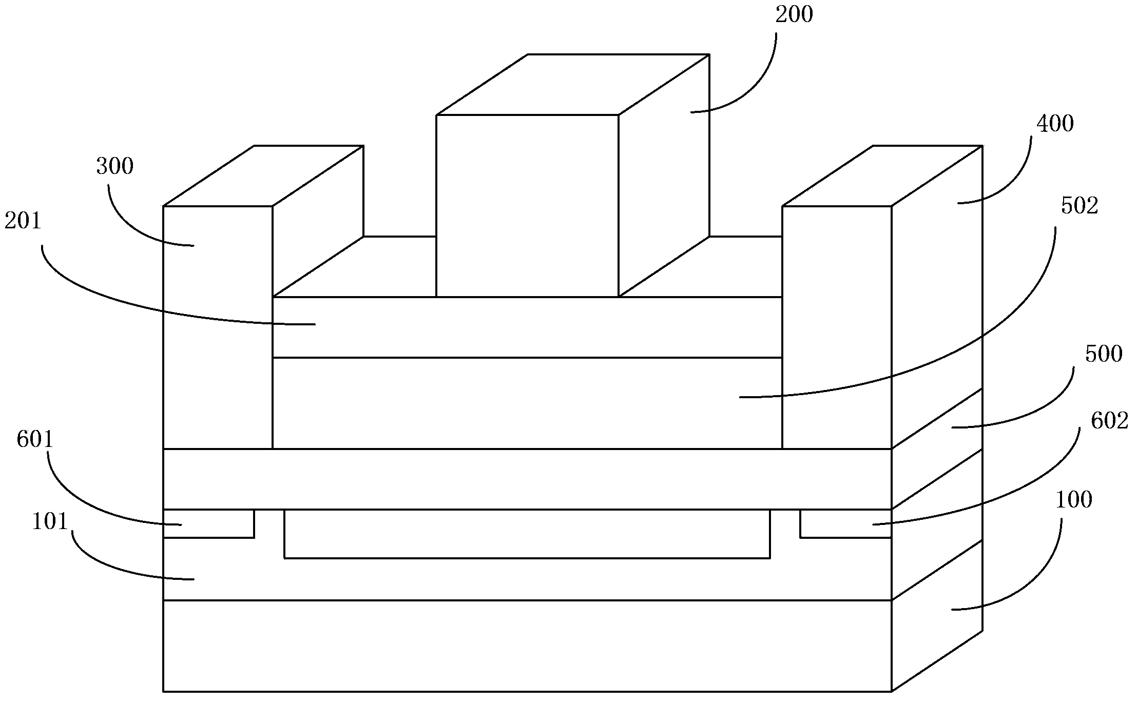
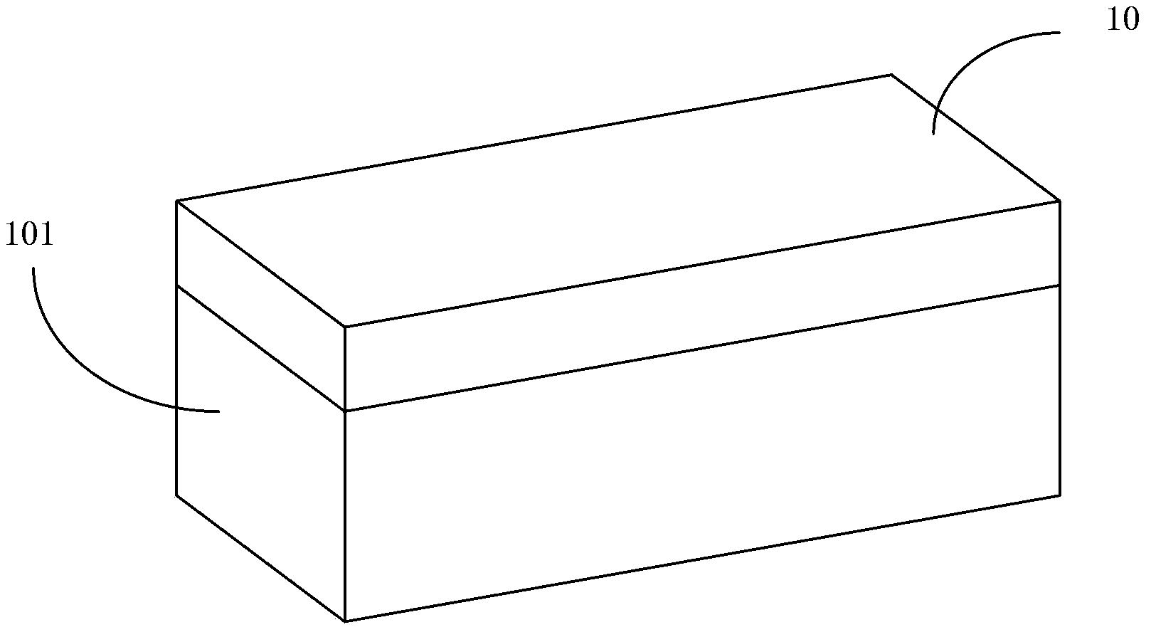
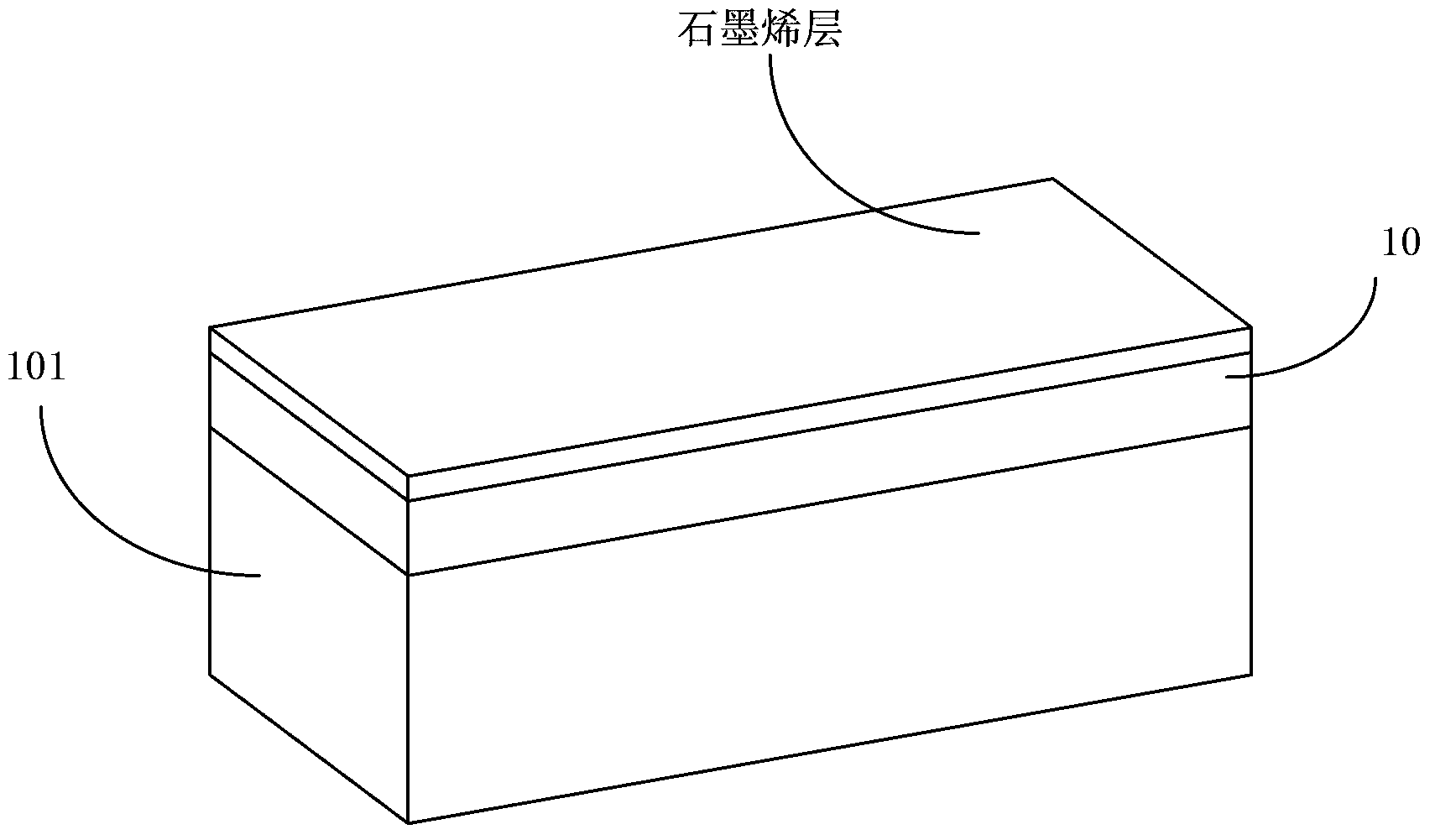
[0013] In the following description, numerous specific details are given in order to provide a more thorough understanding of the present invention. It will be apparent, however, to one skilled in the art that the present invention may be practiced without one or more of these details. In other examples, some technical features known in the art are not described in order to avoid confusion with the present invention.

[0014] Obviously, the practice of the invention is not limited to specific details familiar to those skilled in the semiconductor arts. Preferred embodiments of the present invention are described in detail below, however, the present invention may have other embodiments besides these detailed descriptions.

[0015] It should be understood that when the terms "comprising" and / or "comprising" are used in this specification, they indicate the presence of the features, integers, steps, operations, elements and / or components, but do not exclude the presence or addi...


PUM


Abstract

The invention discloses a double-gate fin-type field effect transistor including a bottom gate, a first dielectric layer on the bottom gate, two bottom contacts at the top part of the first dielectric layer, a fin-type adjustable channel layer on the first dielectric layer and the bottom contacts, a source electrode and a drain electrode, which are formed at positions of the fin-type adjustable channel layer, corresponding to the two bottom contacts, an insulator formed on the fin-type adjustable channel layer and between the source electrode and the drain electrode, a second dielectric layer formed on the insulator and a top gate on the second dielectric layer and a manufacturing method thereof. The double-gate fin-type field effect transistor is provided with the adjustable channel layer, capable of carrying out switch conversion greatly, providing greater channel charge control capability and faster drive current, reducing a short-channel effect and improving performances of contact resistance of a device and the like.

Description

technical field [0001] The present invention relates to the field of semiconductor technology, more precisely, the present invention relates to a double-gate fin field effect transistor and a manufacturing method thereof. Background technique [0002] Graphene is derived from graphite, and its carrier mobility at room temperature is 100 times faster than that of silicon materials, but at the same time, because it is a semiconductor with zero band gap, that is, there is no energy gap between its valence band and conduction band, so if To make semiconductors from this material, then the zero bandgap means that the current switching control of graphene material semiconductors cannot. Solutions to this problem proposed in the prior art include using nanoribbons, quantum dots or chemical methods to modify the graphene material itself to have semiconducting properties. These methods can generally solve the above-mentioned problems, but using these methods to open a band gap in th...

Claims


Application Information

Patent Timeline
IPC IPC(8): H01L29/423H01L29/10H01L29/78H01L21/28H01L21/336
CPCH01L29/78648H01L29/1606H01L29/778H01L29/78603H01L29/78684H01L29/66484H01L29/66795H01L29/7855
Inventor 张海洋王新鹏
Owner SEMICON MFG INT (SHANGHAI) CORP
Why Eureka
Try Eureka