
Preparation method of cuins2 thin film solar cell absorber layer

A technology of solar cells and absorbing layers, applied in circuits, photovoltaic power generation, electrical components, etc., can solve the problems of inability to prepare large-area thin films, high cost, low utilization rate of raw materials, etc., and achieve high utilization rate of raw materials, simple equipment, high yield effect

Inactive Publication Date: 2016-01-27
HARBIN UNIV OF SCI & TECH
View PDF2 Cites 0 Cited by
  • Summary
  • Abstract
  • Description
  • Claims
  • Application Information

AI Technical Summary

Problems solved by technology

[0006] The purpose of the present invention is to solve the problem of preparing CuInS at present 2 Thin-film solar cell absorption layer has high cost, cannot prepare large-area thin film, and the utilization rate of raw materials is not high, and provides CuInS 2 Thin Film Solar Cell Absorber

Method used


Image

  • Preparation method of cuins2 thin film solar cell absorber layer
  • Preparation method of cuins2 thin film solar cell absorber layer
  • Preparation method of cuins2 thin film solar cell absorber layer

Examples


specific Embodiment approach 1

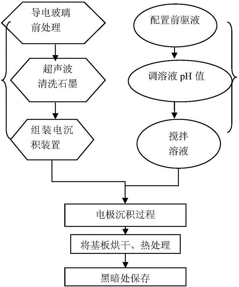
[0031] Specific implementation mode 1: CuInS in this embodiment mode 2 The preparation method of thin-film solar cell absorption layer is carried out according to the following steps:

[0032] 1. The substrate is ultrasonically cleaned with 50% hydrochloric acid, acetone, and absolute ethanol in sequence for 20 to 40 minutes, and then cleaned with distilled water for later use;

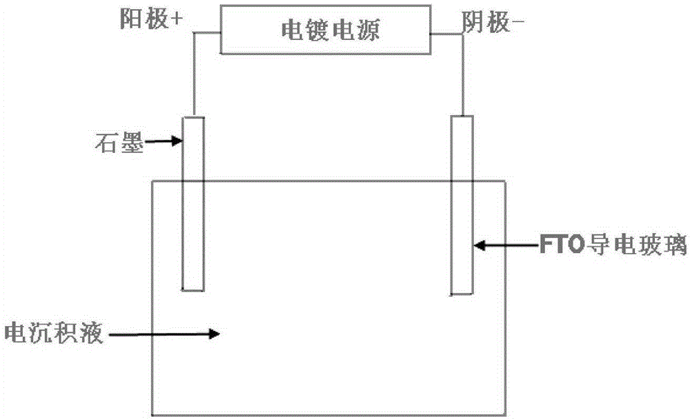
[0033] 2. Electrodeposition of CuInS 2 Film: Take 8~12mmol·L -1 CuSO 4 , 7~8mmol·L -1 In 2 (SO 4 ) 3 , 55~65mmol·L -1 Na 2 S 2 o 3 and 8~9mmol·L -1 C 6 h 5 o 7 Na 3 Prepare an electrolyte solution, and adjust the pH value of the electrolyte solution to 4, then place the substrate cleaned in step 1 in a bipolar electrolytic cell filled with electrolyte solution, perform electrodeposition treatment for 30-60 minutes, take out the substrate, and wash it with distilled water , blow dry;

[0034] 3. Place the electrodeposited substrate in step 2 in a tubular resistance furnace filled with ...

specific Embodiment approach 2

[0035] Embodiment 2: This embodiment differs from Embodiment 1 in that the ultrasonic cleaning time described in Step 1 is 30 minutes. Others are the same as in the first embodiment.

specific Embodiment approach 3

[0036] Specific embodiment three: the difference between this embodiment and specific embodiment one or two is that: get 10mmol L described in step two -1 CuSO 4 , 7.5mmol·L -1 In 2 (SO 4 ) 3 , 60mmol·L -1 Na 2 S 2 o 3 and 8.5mmol·L -1 C 6 h 5 o 7 Na 3 Prepared as an electrolyte. Others are the same as in the first or second embodiment.


PUM


Abstract

The invention discloses a preparation method of an absorbing layer of a CuInS2 thin-film solar cell, relates to the preparation method of the absorbing layer of the solar cell and aims to solve the problems that the cost of an absorbing layer of a CuInS2 thin-film solar cell prepared at the present is high, a large-area film cannot be prepared, and the utilization rate of raw materials is not high. The method comprises the steps as follows: firstly, a substrate is cleaned; secondly, 10 mmol.L-1 of CuSO4, 7.5 mmol.L-1 of In2(SO4)3, 60 mmol.L-1 of Na2S2O3 and 8.5 mmol.L-1 of C6H5O7Na3 are taken and prepared into an electrolyte, and electro-deposition of the substrate is performed; and thirdly, heat treatment of the substrate is performed. An industrial non-vacuum and low-cost CIS2 film is prepared with an electrochemical deposition method. The method of the absorbing layer of the CuInS2 thin-film solar cell is applied to the field of solar cells.

Description

technical field [0001] The invention relates to a method for preparing a solar cell absorbing layer. Background technique [0002] Since the energy problem in the 21st century has attracted great attention from the world, it is imperative to develop and utilize new renewable energy, which is expected to improve the pressure on the world's energy and environment. The development of renewable and clean energy is expected to alleviate the pressure on the world's energy and environment, and it has become a difficult problem that human beings must solve in the 21st century. Therefore, the development of renewable energy has received great attention. [0003] Renewable energy mainly includes water energy, wind energy, tidal energy, geothermal energy and solar energy. Among them, solar energy is praised as "the father of mankind", mainly because of its inexhaustible and inexhaustible advantages; and solar energy will not cause "greenhouse effect", will not produce noise, environme...

Claims


Application Information

Patent Timeline
Patent Type & Authority Patents(China)
IPC IPC(8): H01L31/18H01L31/032
CPCH01L21/02568H01L21/02628H01L31/1876Y02E10/50Y02P70/50
Inventor 李丽波李琦王华林徐妍
Owner HARBIN UNIV OF SCI & TECH
Learn More