

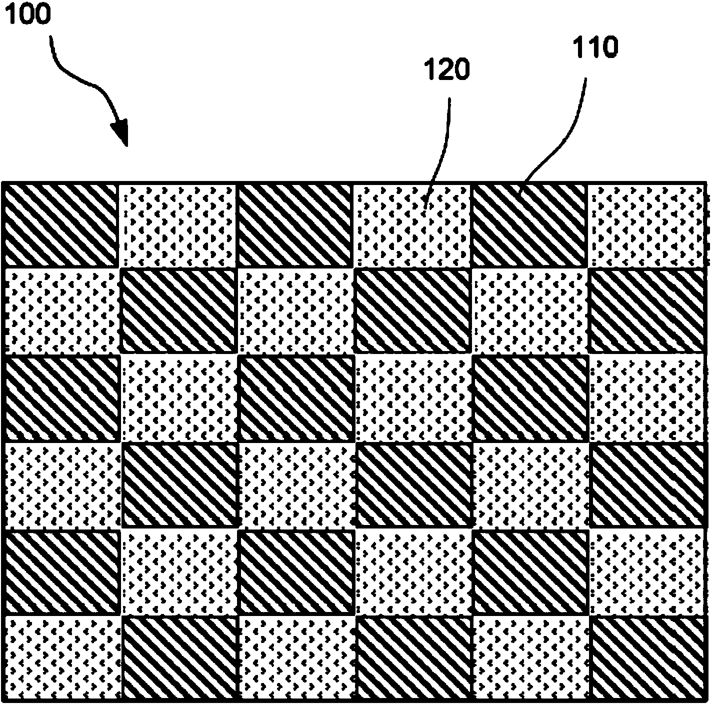
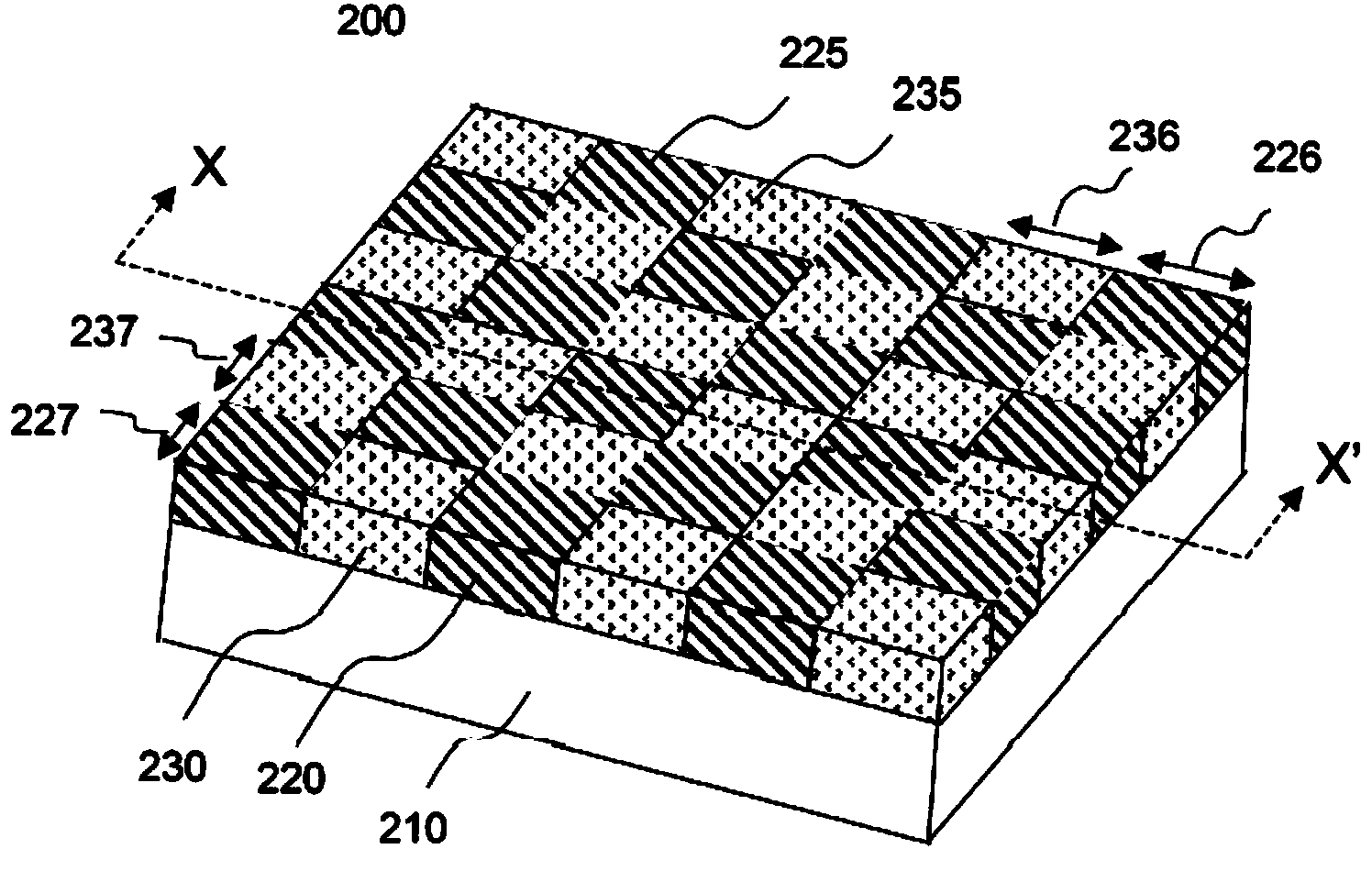
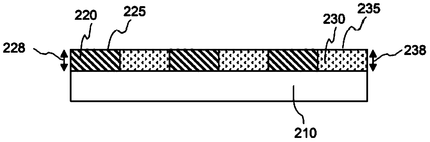
Monitoring network based on nano-structured sensing devices
A nanostructure and detector technology that can be used in nanostructure fabrication, measurement devices, nanotechnology, etc., to solve problems such as difficulty in reproducibly demonstrating enhancement levels
- Summary
- Abstract
- Description
- Claims
- Application Information
AI Technical Summary
Problems solved by technology
Method used
Image

Examples
specific Embodiment approach
[0116] The invention will be further described in the following examples without limiting the scope of the invention described in the claims.
example 1
[0118] Fabrication of nanosurface arrays by anodic oxidation
[0119] Thin films of Ti (about 100 nm) were deposited by electron beam evaporation of silicon (100) wafers, followed by deposition of Ag (about 100 nm). A layer of about 500 nm Al was then deposited on top of the Ag film using physical vapor deposition.
[0120] The coated Si wafer was then put into an anodic oxidation plating bath with about 0.3M oxalic acid solution as electrolytic solution. The electroplating bath was maintained at about 10°C, and the anodizing voltage was set at about 35V. After anodization, nanometer-sized narrow pores in the Al 2 o 3 formed in the layer. The diameter of the pores (or holes) can be widened by placing the wafer in about 10 wt.% phosphoric acid solution. Al 2 o 3 The nanoporous structure in the layer acts as a mask for etching the active metal layer or depositing the active metal layer. In this way, nanosurface arrays were formed after removal of the oxidized Al layer. ...
example 2
[0122] Nanoimprint lithography for fabrication of nanosurface arrays
[0123] The first step in nanoimprinting is to imprint a mold into a thin resist cast on a substrate. The purpose of this step is to replicate the nanostructures on the mold into the resist film. The second step is to etch the resist film to form nanostructures on the substrate.
[0124] Using electron beam lithography and reactive ion etching (RIE) on a Si wafer, the mold was patterned with an array of nanodots with a feature size of 30 nm. PMMA was used as resist on Au-coated Si(100) wafers. A thin Ti layer is inserted between Au and Si to enhance adhesion. The imprinting process is carried out in a vacuum at a pressure of about 1000 Pascals (psi) at about 160 °C above the glass transition temperature of PMMA. After the pattern from the mold was transferred to the Au-coated Si (100), oxidative reactive ion etching (RIE) was used to remove the residual resist in the PMMA pinched areas. Then, the patter...
PUM
| Property | Measurement | Unit |
|---|---|---|
| height | aaaaa | aaaaa |
| width | aaaaa | aaaaa |
| size | aaaaa | aaaaa |
Abstract
Description
Claims
Application Information