
Plant illumination device and method

A lighting device and lighting method technology, applied in the directions of botanical equipment and methods, horticultural methods, greenhouse cultivation, etc., can solve the problems of not allowing emission spectrum analysis and tuning, poor main light source, poor quality harvests, etc., and achieve improved light form Form control, excellent energy efficiency, and optimal spectral tuning

Inactive Publication Date: 2014-02-05
VALOYA
View PDF6 Cites 11 Cited by
  • Summary
  • Abstract
  • Description
  • Claims
  • Application Information

AI Technical Summary

Problems solved by technology

Prior art fluorescent tube, LED and phosphor configurations do not allow sufficiently high resolution tuning of the emission spectrum
In addition, prior art fluorescent tube, LED and phosphor configurations are poor primary light sources for plants, producing poor quality harvests in dark growing chambers such as basements of buildings, etc.

Method used


Image

  • Plant illumination device and method
  • Plant illumination device and method
  • Plant illumination device and method

Examples


Embodiment Construction

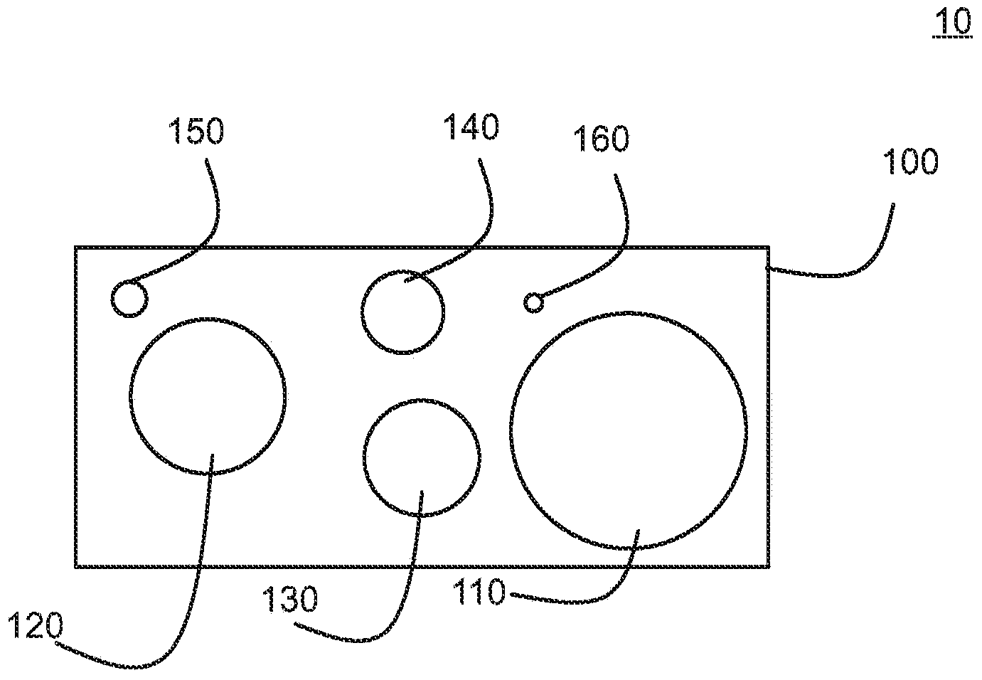
[0075] Figure 1B Illumination device 100 is shown comprising a plurality of quantum dots 110, 120, 130, 140, 150 and 160 of different sizes. The size distribution of quantum dots comprises quantum dots of different sizes in the range of 2nm to 200nm, ie quantum dots 110 typically have a diameter of 200nm and quantum dots 160 have a diameter of about 2nm.

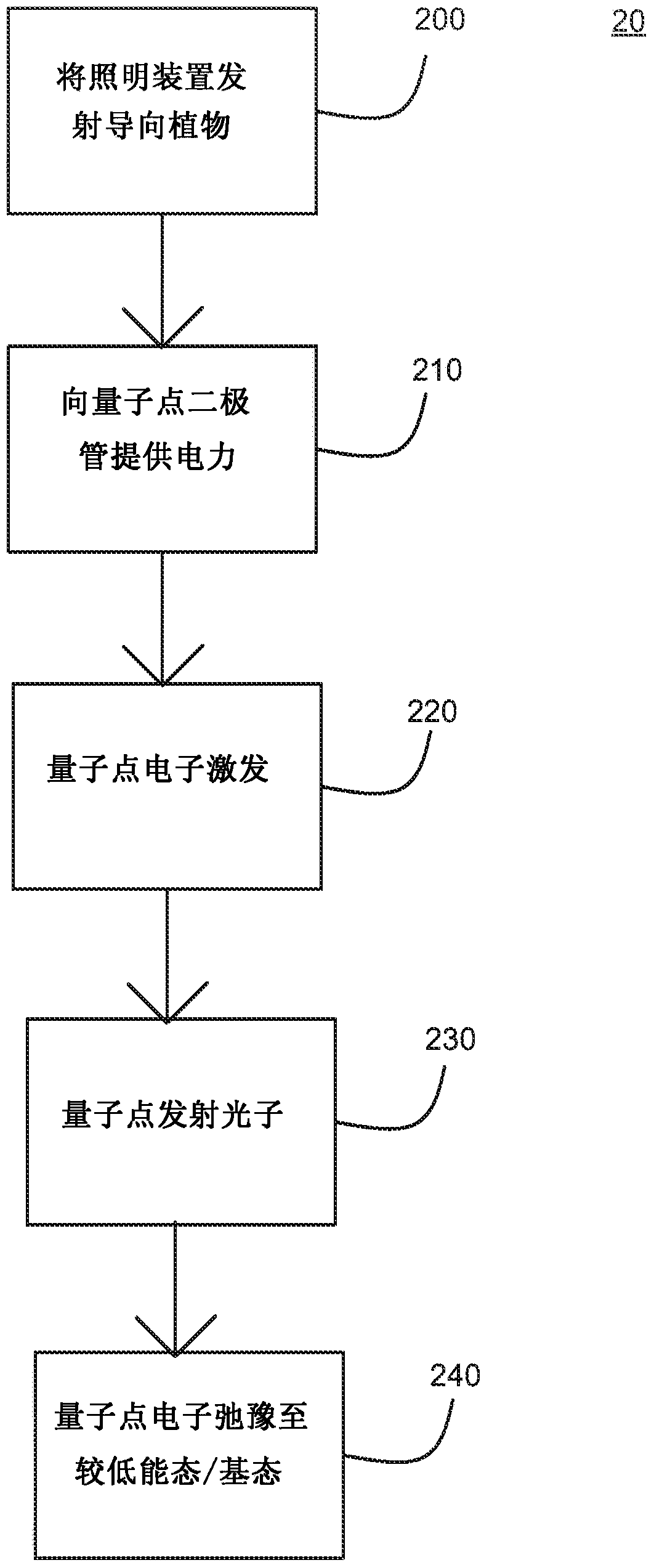
[0076] Electric power and electrodes (not shown) are used to generate an electric field to excite electrons in the quantum dots in a conventional manner. As an electron relaxes to a lower energy state, it emits a photon whose wavelength is determined by the energy difference between the excited and relaxed state. These emitted photons generate the emission spectrum of the lighting device 100 .

[0077] In some embodiments, quantum dots 150, 160 are configured to transmit UV / blue light in the range of 250nm to 400nm, quantum dots 140 and 130 are configured to transmit green and / or yellow light from 400nm to 600nm, and quan...


PUM

PropertyMeasurementUnit
Fwhmaaaaaaaaaa

Abstract

The invention relates to an improved method to produce artificial light for plant cultivation. In more particular, the invention relates to an illumination device with a semiconductor light emission solution and device suited for plant cultivation in a greenhouse environment. The best mode of the invention is considered to be a lighting device with binary alloy quantum dots (110, 120, 130, 140, 150, 160) made by colloidal methods to produce a size distribution of quantum dots that produces an emission spectrum similar to the photosynthetically active radiation (PAR) spectrum. The methods and arrangements of the invention allow more precise spectral tuning of the emission spectrum for lights used in plant (310, 311) cultivation. The invention therefore realises unexpected improvements in the photomorphogenetic control of plant growth, and further improvements in plant production.

Description

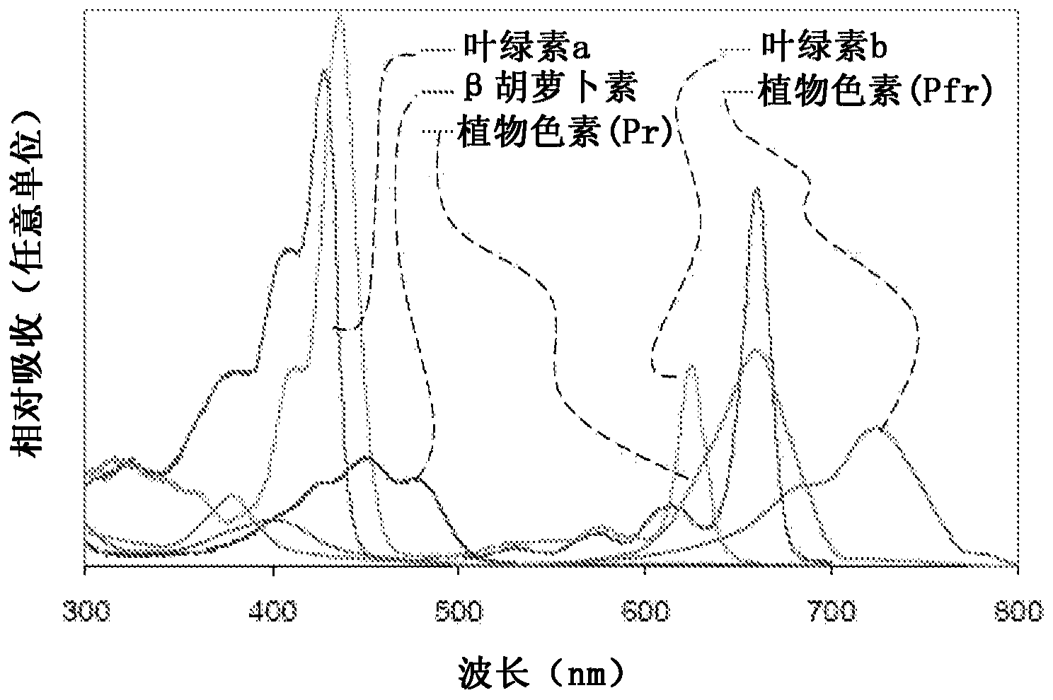
technical field [0001] The present invention relates to an improved method of producing artificial light for plant cultivation. More specifically, the present invention relates to a lighting device having a semiconductor light emitting scheme suitable for plant cultivation in a greenhouse environment. Background technique [0002] Only about 50% of the radiation reaching the ground is photosynthetically active radiation (PAR). PAR is interpreted as encompassing the wavelength range between 300nm and 800nm ​​of the electromagnetic spectrum. Photosynthesis and photoperiodism, phototropism and photomorphogenesis are four representative processes related to the interaction between radiation and plants. The following expression shows a simplified chemical equation for photosynthesis: [0003] 6H 2 O+6CO 2 (+photon energy)→C 6 h 12 o 6 +6O 2 . [0004] Figure 1A The two interconvertible forms of the most common photosynthetic and photomorphogenic photoreceptors (such as...

Claims


Application Information

Patent Timeline
IPC IPC(8): H01L33/06A01G7/04
CPCA01G7/045H01L33/06A01G9/249Y02P60/14A01G9/20H01L33/504
Inventor 拉尔斯·艾卡拉伊尔卡·基维马基
Owner VALOYA
Learn More