Metallizing method for chip front electrode and auxiliary devices

A front electrode and auxiliary device technology, applied in the direction of metal material coating process, circuit, electrical components, etc., can solve the problems of harsh operating environment, complex process steps, and the packaging workshop cannot meet the requirements, and achieve the requirements of reducing the operating environment, The effect of simplifying the machining process

Inactive Publication Date: 2014-02-12
INST OF ELECTRICAL ENG CHINESE ACAD OF SCI
View PDF6 Cites 9 Cited by
  • Summary
  • Abstract
  • Description
  • Claims
  • Application Information

AI Technical Summary

Problems solved by technology

[0011] 1. The process steps are complicated, requiring equipment such as glue homogenizer and photolithography machine;
[0012] 2. The

Method used


Image

  • Metallizing method for chip front electrode and auxiliary devices
  • Metallizing method for chip front electrode and auxiliary devices
  • Metallizing method for chip front electrode and auxiliary devices

Examples


Embodiment Construction

[0035] The technical solutions in the embodiments of the present invention will be clearly and completely described below in conjunction with the accompanying drawings in the embodiments of the present invention. Obviously, the described embodiments are only some, not all, embodiments of the present invention. Based on the embodiments of the present invention, all other embodiments obtained by persons of ordinary skill in the art without creative efforts fall within the protection scope of the present invention.

[0036] The invention provides a method and an auxiliary device for metallizing the front electrode of a chip to simplify the chip processing technology.

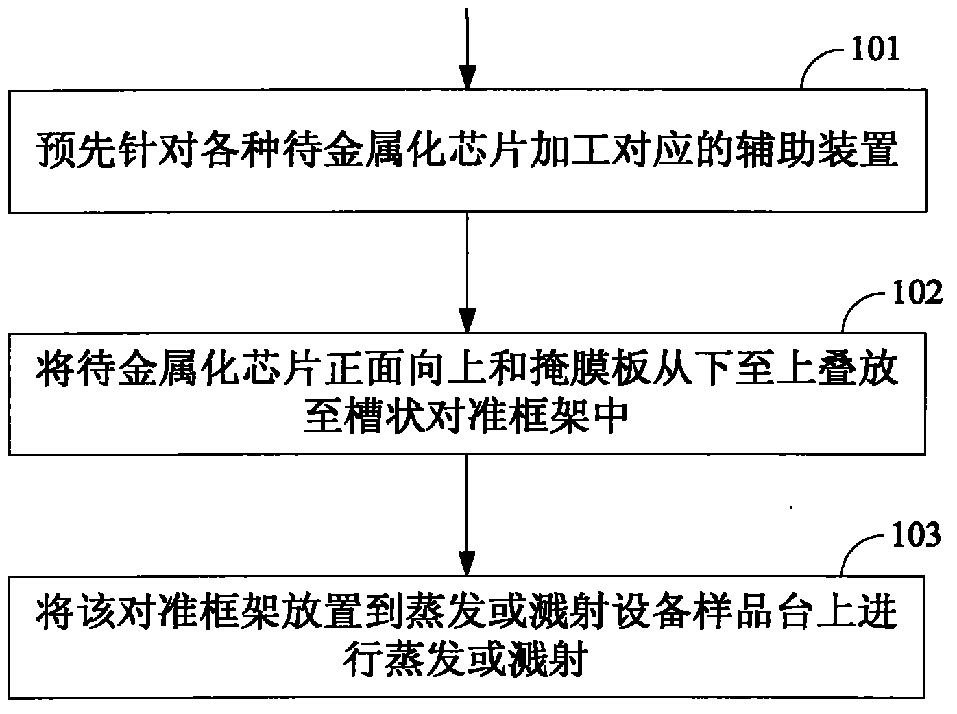
[0037] Such as figure 1 As shown, a preferred embodiment of the method for chip front electrode metallization of the present invention comprises the following steps:

[0038] Step 101 , processing corresponding auxiliary devices for various chips to be metallized in advance.

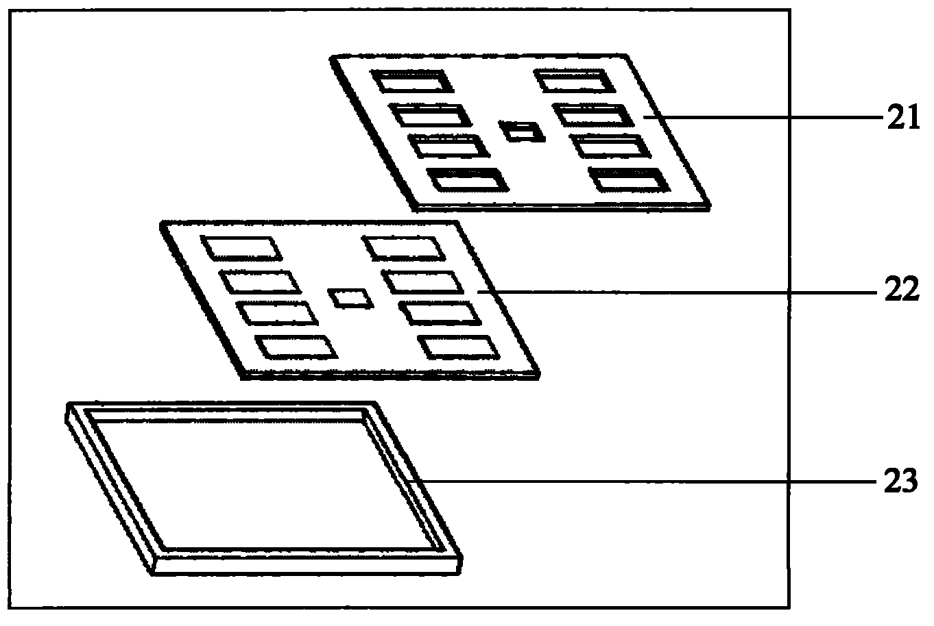
[0039] Such as figure 2 As shown, ...


PUM


Abstract

The invention discloses a metallizing method for a chip front electrode. The method comprises the steps: A, stacking up a to-be-metallized chip with the front surface upward and a mask plate from bottom to top into a groove-shaped alignment frame, and enabling the pattern of the chip front electrode to be completely aligned to the hollowed electrode pattern in the mask plate; B, placing the alignment frame to evaporating or sputtering equipment for carrying out evaporating or sputtering, and generating a needed metal layer on the pattern of the chip front electrode. The invention discloses two auxiliary devices used for the method. The auxiliary devices comprise the mask plates and the groove-shaped alignment frame. By applying the method and the auxiliary devices, the processing technology of metallizing the chip front electrode can be simplified, and the requirement for the operation environment by processing is lowered.

Description

technical field [0001] The invention relates to a semiconductor processing technology, in particular to a method and an auxiliary device for metallizing a front electrode of a chip. Background technique [0002] With the development of semiconductor technology, module packaging technology with double-sided cooling structure has emerged. This packaging method can improve the heat dissipation function of modules, especially power semiconductor modules, such as insulated gate bipolar transistor (IGBT) modules. [0003] In the IGBT chip, the gate and emitter are on the front side, and the back side of the chip is the collector. The new double-sided cooling package requires that the front electrode of the chip should be connected to other parts of the module, such as the DBC copper clad layer, by soldering, not only to achieve electrical connection, but also to achieve heat dissipation. The front electrode of the existing chip uses an aluminum electrode. The aluminum electrode c...

Claims


Application Information

Patent Timeline
IPC IPC(8): H01L21/285C23C14/04
CPCH01L21/2855C23C14/042
Inventor 靳鹏云郑利兵韩立王春雷方化潮
Owner INST OF ELECTRICAL ENG CHINESE ACAD OF SCI
Why Eureka
Try Eureka