
A kind of flip-chip structure light-emitting diode and its preparation method

A light-emitting diode, flip-chip technology, applied in electrical components, circuits, semiconductor devices, etc., can solve the problems of mismatch of thermal expansion coefficients of polymer layers, the risk of isolation of insulating film 212, and leakage of LED structure sidewalls. The effect of reducing the probability, eliminating the possibility, and improving the reliability

Active Publication Date: 2016-12-21
TONGFANG OPTO ELECTRONICS +1
View PDF6 Cites 0 Cited by
  • Summary
  • Abstract
  • Description
  • Claims
  • Application Information

AI Technical Summary

Problems solved by technology

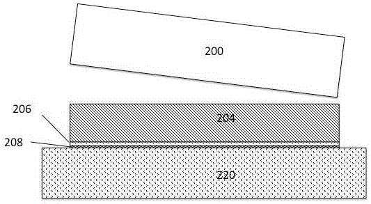
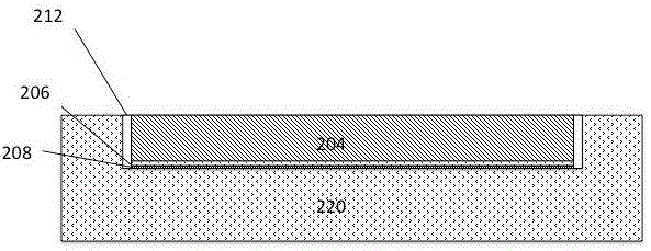
In the actual manufacturing process, after the sapphire substrate 200 is peeled off by laser, the insulating film 212 near the peeling interface is easily damaged by the impact of laser energy. In addition, the support substrate 220 is used, and the surface may also be instantly heated by the laser to produce a liquid state. The melting phenomenon makes the isolation of the insulating film 212 in the horizontal direction on the peeling interface risky, so it is necessary to use a very thick sidewall insulating film 212 to prevent leakage. In the actual coating process, silicon oxide with a thickness of several um is plated Or the silicon nitride film is very difficult and costly, the polymer layer is too wide and there are problems of secondary light absorption and thermal expansion coefficient mismatch, so that the vertical LED structure has always had the problems of side wall leakage and poor reliability

Method used


Image

  • A kind of flip-chip structure light-emitting diode and its preparation method
  • A kind of flip-chip structure light-emitting diode and its preparation method
  • A kind of flip-chip structure light-emitting diode and its preparation method

Examples


Embodiment Construction

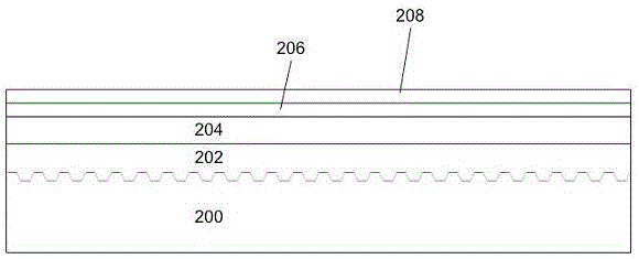
[0029] see Figure 9 The structure of the present invention includes a metal support substrate 220, an N-type ohmic contact metal layer 218, an insulating film 212, a reflective metal layer 210, a P-type semiconductor layer 208, a quantum well light-emitting layer 206, and an N-type semiconductor layer stacked in sequence from bottom to top. 204 and undoped layer 202. Multiple layers of metal are placed on and around the reflective metal layer 210 and extend to the side to serve as a P-type electrode 214 . The metal support substrate 220 is connected to the N-type semiconductor layer 204 and the non-doped layer 202 to form an N-type electrode.

[0030] see Figure 3 to Figure 9 , the steps of the preparation method of the flip-chip light-emitting diode of the present invention are:

[0031] Select a patterned sapphire substrate 200, and grow an epitaxial layer with a thickness of 3~10 um on the sapphire substrate 200 with metal-organic chemical vapor deposition equipment. ...


PUM


Abstract

The invention discloses a light-emitting diode of an inversion structure and a manufacturing method of the light-emitting diode of the inversion structure, and relates to the field of the photoelectric technology. The light-emitting diode comprises a metal supporting substrate, a P-type semiconductor layer, a quantum well light-emitting layer, an N-type semiconductor layer and a non-doped layer which are sequentially overlapped from bottom to top. The light-emitting diode is structurally characterized in that an N-type ohmic contact metal layer, an insulating film and a reflection metal layer are arranged between the metal supporting substrate and the P-type semiconductor layer, multiple layers of metal are arranged above and around the reflection metal layer and extend to the side to serve as a P-type electrode, the metal supporting substrate is connected with the N-type semiconductor layer through the N-type ohmic contact metal layer to serve as an N-type electrode. Compared with the prior art, the light-emitting diode of the inversion structure and the manufacturing method of the light-emitting diode of the inversion structure can effectively avoid electricity leakage of the lateral wall of a chip of the light-emitting diode, improve the reliability of the chip, reserve the advantages of an original vertical-type LED structure, and give the efficiency of the vertical-type LED structure into full play.

Description

technical field [0001] The invention relates to the field of optoelectronic technology, in particular to a light-emitting diode with an inverted structure and a preparation method thereof. Background technique [0002] At present, in light-emitting diodes (LEDs) made of Ga(Al,In)N semiconductor materials, such as US Patent No. 7,763,477B2 and other documents, the flip-chip LED structure is close to the substrate with high heat dissipation due to the semiconductor junction. Compared with the traditional front-mount LED, the chip structure with sapphire as the substrate has higher reliability and greater operating power, and has received great attention and research. [0003] In the prior art, the latest flip-chip LED chip structure uses substrate replacement technology to flip-chip the epitaxy on a new conductive and thermally conductive metal support substrate 220, and remove the original sapphire substrate 200, such as figure 1 shown. With the thicker N-type semiconductor...

Claims


Application Information

Patent Timeline
Patent Type & Authority Patents(China)
IPC IPC(8): H01L33/48H01L33/60H01L33/36
CPCH01L33/405H01L33/60H01L33/647
Inventor 郑兆祯朱俊宜郭德博涂庆明
Owner TONGFANG OPTO ELECTRONICS
Learn More