Space overlaid and coupled high-power semiconductor laser stack array system

A space coupling, semiconductor technology, applied in the laser field, can solve problems such as complex process, achieve the effect of simple and compact structure, easy installation and debugging, and stable performance

Inactive Publication Date: 2014-02-12
NORTHWEST UNIV(CN)
View PDF5 Cites 15 Cited by
  • Summary
  • Abstract
  • Description
  • Claims
  • Application Information

AI Technical Summary

Problems solved by technology

Effectively solves the complexity problem of the existing semiconductor laser technology, and outputs high-power strip-shaped uniform spot

Method used


Image

  • Space overlaid and coupled high-power semiconductor laser stack array system
  • Space overlaid and coupled high-power semiconductor laser stack array system
  • Space overlaid and coupled high-power semiconductor laser stack array system

Examples


Embodiment

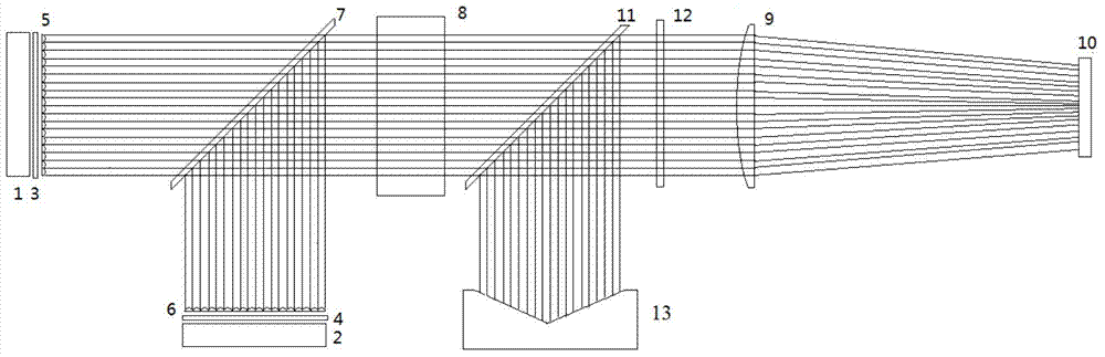
[0045] Following the technical solution of the present invention, the space superposition coupled high-power semiconductor laser array system of this embodiment includes a first semiconductor laser array 1, a second semiconductor laser array 2, a first fast-axis collimating lens group 3, a first Two fast-axis collimating lens groups 4, first slow-axis collimating lens array group 5, second slow-axis collimating lens array group 6, periodic space coupling mirror 7, slow-axis beam expander system 8, focusing mirror 9 , a polarizer 11 , a quarter wave plate 12 and a light blocker 13 . in:

[0046] The first semiconductor laser stack 1 and the second conductor laser stack 2 are the same, and they all use a 3000-watt stack formed by stacking 25 semiconductor laser bars with a power of 976 nm and a power of 120 W along the fast axis direction. The total power of the first semiconductor laser array 1 and the second conductor laser array 2 is 6000 watts. like image 3 As shown in t...


PUM


Abstract

The invention discloses a space overlaid and coupled high-power semiconductor laser stack array system. The space overlaid and coupled high-power semiconductor laser stack array system comprises a first semiconductor laser stack array and a second semiconductor laser stack array which are respectively formed by overlaying a plurality of semiconductor labor diode bars in the direction of a fast axis, wherein the number of the diode bars of the first semiconductor laser stack array is equal to the number of the diode bars of the second semiconductor laser stack array. The space overlaid and coupled high-power semiconductor laser stack array system further comprises a first fast axis collimating lens set, a second fast axis collimating lens set, a first slow axis collimating lens array set, a second slow axis collimating lens array set, a periodical space coupling lens, a slow axis beam expanding system and a focus lens. The two laser stack arrays in the system are overlapped in the space through a periodical space coupling lens to output a high-power laser, the beam collimation is achieved through the fast axis collimating lenses and the slow axis collimating lenses, the characteristics of high brightness and linear polarization are kept, and meanwhile internal components are protected through an added feedback optical isolation system. The problem that the existing semiconductor laser technology is complex is effectively solved, and even high-power and strip-shaped light spots are output.

Description

technical field [0001] The invention belongs to the technical field of lasers, and in particular relates to a space superposition coupled high-power semiconductor laser stacked array system. Background technique [0002] Due to the high brightness, high power density, small thermal action area, short material processing time, fast processing speed, non-contact processing, no "tool" wear, and no "cutting force" acting on the workpiece, the laser can treat a variety of metals and non-metals. Processing, especially high hardness, high brittleness and high melting point materials and CNC system to form a laser processing center, small heat affected zone, small workpiece deformation, small follow-up processing, high production efficiency, stable and reliable processing quality, solving many conventional methods can not be. The problems solved have greatly improved work efficiency and processing quality. At present, the manufacturing industry in developed countries has entered the...

Claims


Application Information

Patent Timeline
Patent Type & Authority Applications(China)
IPC IPC(8): H01S5/40H01S5/06
Inventor 王春白晋涛任兆玉冯晓强曹勇王思原张伯阳
Owner NORTHWEST UNIV(CN)
Why Eureka
Try Eureka