Method for making flexible, transparent and conductive film made of metal nanowires

A transparent conductive film, metal nanowire technology, applied in nanotechnology, cable/conductor manufacturing, semiconductor/solid-state device manufacturing, etc., can solve problems such as poor environmental stability, large surface roughness, limited application, etc., to solve the adhesion force Poor, high surface flatness, solve the effect of large surface roughness

Inactive Publication Date: 2014-02-19
CHANGCHUN INST OF OPTICS FINE MECHANICS & PHYSICS CHINESE ACAD OF SCI
View PDF9 Cites 24 Cited by
  • Summary
  • Abstract
  • Description
  • Claims
  • Application Information

AI Technical Summary

Problems solved by technology

However, metal nanowire transparent conductive films based on flexible substrates also have obvious shortcomings such as large surface roughness, low adhesion, and poor environmental stability, which severely limit their applications in optoelectronic devices.

Method used


Image

  • Method for making flexible, transparent and conductive film made of metal nanowires
  • Method for making flexible, transparent and conductive film made of metal nanowires
  • Method for making flexible, transparent and conductive film made of metal nanowires

Examples


preparation example Construction

[0029] Specifically, the preparation method of the metal nanowire flexible transparent conductive film of the present invention comprises the following steps:

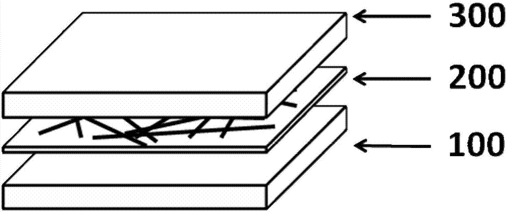
[0030] First, metal nanowire solutions with different concentrations are prepared, and a metal nanowire layer 200 with a thickness of 30-300 nm is prepared on a planar substrate 100 by a solution processing method; 500 μm transparent flexible base layer 300; finally, the transparent flexible base layer 300 with the metal nanowire layer 200 on the surface is peeled off from the planar substrate 100 to form a metal nanowire flexible transparent conductive film.

[0031] The above-mentioned planar substrate 100 is rigid material such as glass, quartz or semiconductor.

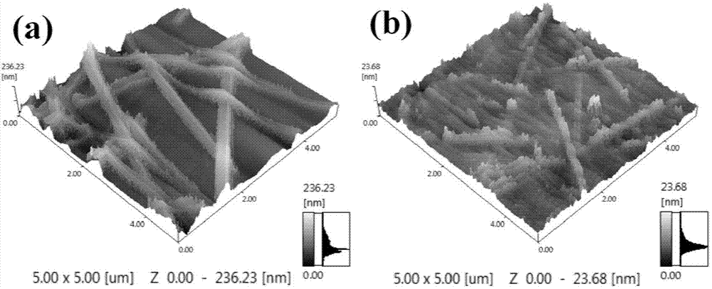
[0032] The above-mentioned metal nanowire solution is a nanowire dispersion liquid of metal materials such as Ag, Au or Cu, the diameter of the metal nanowire is 30-200nm, the length is 5-30μm, and the solution concentration is 0.1-6mg / ml.

[0033] The ab...

Embodiment 1

[0038] A metal nanowire layer 200 with a thickness of 60 nm is prepared on a flat substrate 100 by a drop coating method, and a transparent flexible base layer 300 with a thickness of 25 μm is prepared on the metal nanowire layer 200 by a drop coating method, and finally the surface is covered with metal nanowires. The transparent and flexible base layer 300 of the wire layer 200 is peeled off from the planar substrate 100 to form a flexible transparent conductive film of metal nanowires. The planar substrate 100 is a glass substrate; the metal nanowire layer 200 is prepared from a silver nanowire solution with a concentration of 1 mg / ml, the diameter of the metal silver nanowire is 50 nm, and the length is 15 μm; the transparent flexible base layer 300 is a PI substrate.

Embodiment 2

[0040] A metal nanowire layer 200 with a thickness of 100 nm is prepared on a flat substrate 100 by a drop coating method, and a transparent flexible base layer 300 with a thickness of 25 μm is prepared on the metal nanowire layer 200 by a drop coating method, and finally the surface is coated with metal nanowires. The transparent and flexible base layer 300 of the wire layer 200 is peeled off from the planar substrate 100 to form a flexible transparent conductive film of metal nanowires. The planar substrate 100 is a glass substrate; the metal nanowire layer 200 is prepared from a silver nanowire solution with a concentration of 2 mg / ml, and the diameter of the metal silver nanowire is 50 nm, and the length is 15 μm; the transparent flexible base layer 300 is a PI substrate.


PUM

PropertyMeasurementUnit
diameteraaaaaaaaaa
lengthaaaaaaaaaa
thicknessaaaaaaaaaa

Abstract

The invention provides a method for making a flexible, transparent and conductive film made of metal nanowires, and belongs to the technical field of conductive film materials. A layer of metal nanowire film is made on a rigid plane substrate according to a solution processing method, then a layer of transparent and flexible substrate is made on the metal nanowire film according to the solution processing method, and finally the flexible substrate with the metal nanowires on the surface is removed from the plane substrate to form the flexible, transparent and conductive film made of the metal nanowires. Compared with a traditional flexible, transparent and conductive film made of metal nanowires directly on a flexible substrate, the flexible, transparent and conductive film made of the metal nanowires through the method has the advantages of being high in surface flatness, large in adhesion force and the like and effectively solving the problems that a flexible, transparent and conductive film made of metal nanowires is large in roughness and small in adhesion force. The flexible, transparent and conductive film made of the metal nanowires has the potential of being applied in the fields of photoelectric devices like film solar cells and organic light-emitting diodes.

Description

technical field [0001] The invention relates to the technical field of transparent conductive film materials, in particular to a method for preparing a metal nanowire flexible transparent conductive film. Background technique [0002] Transparent conductive film is an important optoelectronic functional film, which is widely used in optoelectronic devices such as liquid crystal display, organic light emitting diode, touch screen and thin film solar cell. With the improvement of performance and its rapid development in terms of low cost, flexibility and light weight, optoelectronic devices also put forward higher requirements for the performance of transparent conductive films. At present, the most commonly used and commercialized transparent conductive film is indium tin oxide (ITO) film, which has high visible light transmittance and low resistivity, and is often used in organic solar cells and organic light-emitting diodes, etc. As a transparent electrode in optoelectroni...

Claims


Application Information

Patent Timeline
Patent Type & Authority Applications(China)
IPC IPC(8): H01B13/00H01L51/48B82Y40/00
CPCY02E10/549
Inventor 郭晓阳刘星元
Owner CHANGCHUN INST OF OPTICS FINE MECHANICS & PHYSICS CHINESE ACAD OF SCI
Why Eureka
Try Eureka