Preparation method of crystalline silicon solar cell passive film

A solar cell and passivation film technology, which is applied in circuits, photovoltaic power generation, electrical components, etc., can solve the problems of multiple impurities, dislocations and grain boundaries, low output power of polycrystalline silicon solar cells, and unsatisfactory passivation effect on the surface of silicon wafers, etc. problems, to achieve the effect of increasing output power and reducing impurities

Inactive Publication Date: 2014-03-12
RENESOLA JIANGSU LTD
View PDF3 Cites 3 Cited by
  • Summary
  • Abstract
  • Description
  • Claims
  • Application Information

AI Technical Summary

Problems solved by technology

[0004] However, the passivation effect of the existing anti-reflection film on the surface of the silicon wafer is not ideal, and there are still many defects such as impurities, dislocations and grain boundaries on the surface of the silicon wafer, which makes the output power of polycrystalline silicon solar cells lower

Method used


Image

  • Preparation method of crystalline silicon solar cell passive film

Examples


preparation example Construction

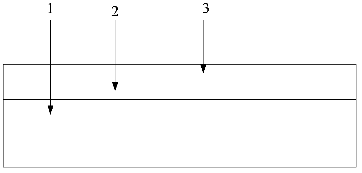
[0036] To this end, the invention discloses a method for preparing a passivation film for a crystalline silicon solar cell, comprising: pretreating a silicon wafer, forming an a-Si:H thin film on the surface of the silicon wafer, and forming an a-Si:H film on the surface of the a-Si: A SiNx:H film is formed on the surface of the H film and sintered.

[0037] As can be seen from the above scheme, the present application first forms a film layer on the surface of the silicon wafer mainly based on H, which plays a certain passivation effect on the surface of the silicon wafer, and then forms a SiNx:H thin film, and the H in the SiNx:H thin film It can play the role of secondary passivation on the surface of the silicon wafer, so that the passivation of the surface of the silicon wafer is more sufficient, and the defects such as impurities, dislocations and grain boundaries on the surface of the silicon wafer are reduced as much as possible. Compared with the existing anti-reflecti...


PUM

PropertyMeasurementUnit
thicknessaaaaaaaaaa
thicknessaaaaaaaaaa
thicknessaaaaaaaaaa

Abstract

The invention provides a preparation method of a crystalline silicon solar cell passive film. The preparation method comprises that: a silicon chip is preprocessed, an a-Si:H thin film is formed on the surface of the silicon chip, a SiNx:H thin film is formed on the surface of the a-Si:H thin film, and sintering is performed. That is to say, firstly, a film layer is formed on the surface of the silicon chip with H as the primary part so that certain passivation effect on the surface of the silicon chip is realized, then the SiNx:H thin film is formed. Besides, H in the SiNx:H thin film has an effect of secondary passivation on the surface of the silicon chip so that passivation on the surface of the silicon chip is fully realized, and defects of impurities, dislocation and crystal boundaries on the surface of the silicon chip are reduced as much as possible. Compared with existing antireflection films, the defects of impurities, dislocation and crystal boundaries existing on the surface of the silicon chip can be effectively reduced by the method provided by the application so that output power of crystalline silicon solar cells is enhanced.

Description

Technical field: [0001] The invention relates to the technical field of solar cell manufacturing, in particular to a method for preparing a passivation film of a crystalline silicon solar cell. Background technique: [0002] Crystalline silicon solar cells can convert light energy into electrical energy, which is a key point in the development of a modern energy-saving society. [0003] During the manufacturing process of polysilicon solar cells, an anti-reflection film is usually formed on the surface of the silicon wafer. The material of the anti-reflection film is generally silicon nitride, which is used to reduce the reflection of light on the surface of polysilicon solar cells, thereby improving its photoelectric conversion efficiency. Generally, the preparation method of the anti-reflection film in the prior art is: passing ammonia gas and silane into the deposition chamber of PECVD (Plasma Enhanced Chemical Vapor Deposition, plasma enhanced chemical vapor deposition) ...

Claims


Application Information

Patent Timeline
Patent Type & Authority Applications(China)
IPC IPC(8): H01L31/18H01L31/0216
CPCH01L31/02167Y02E10/50Y02P70/50
Inventor 汤丹王立建
Owner RENESOLA JIANGSU LTD
Why Eureka
Try Eureka