Method for manufacturing junction barrier schottky diode through selective oxidation of silicon

A junction barrier Schottky and selective oxidation technology, which is applied in semiconductor/solid-state device manufacturing, electrical components, circuits, etc., can solve the problem of reducing forward current, reducing the function and efficiency of forward conduction current, and the area of ​​conduction current Smaller and other problems, to achieve the effect of compensating area, improving function and efficiency, and increasing conductive area

Active Publication Date: 2014-03-26
桂林斯壮桂微电子有限责任公司
View PDF5 Cites 13 Cited by
  • Summary
  • Abstract
  • Description
  • Claims
  • Application Information

AI Technical Summary

Problems solved by technology

However, the disadvantage of this barrier Schottky diode is that the added "P" or "N" type island region occupies a part of the area of ​​the original Schottky barrier interface; so in the case of forwar

Method used


Image

  • Method for manufacturing junction barrier schottky diode through selective oxidation of silicon
  • Method for manufacturing junction barrier schottky diode through selective oxidation of silicon
  • Method for manufacturing junction barrier schottky diode through selective oxidation of silicon

Examples


Embodiment 1

[0028] A method for manufacturing a junction barrier Schottky diode using a silicon selective oxidation technique, comprising a crystal generating step and a packaging step, wherein the crystal generating step includes:

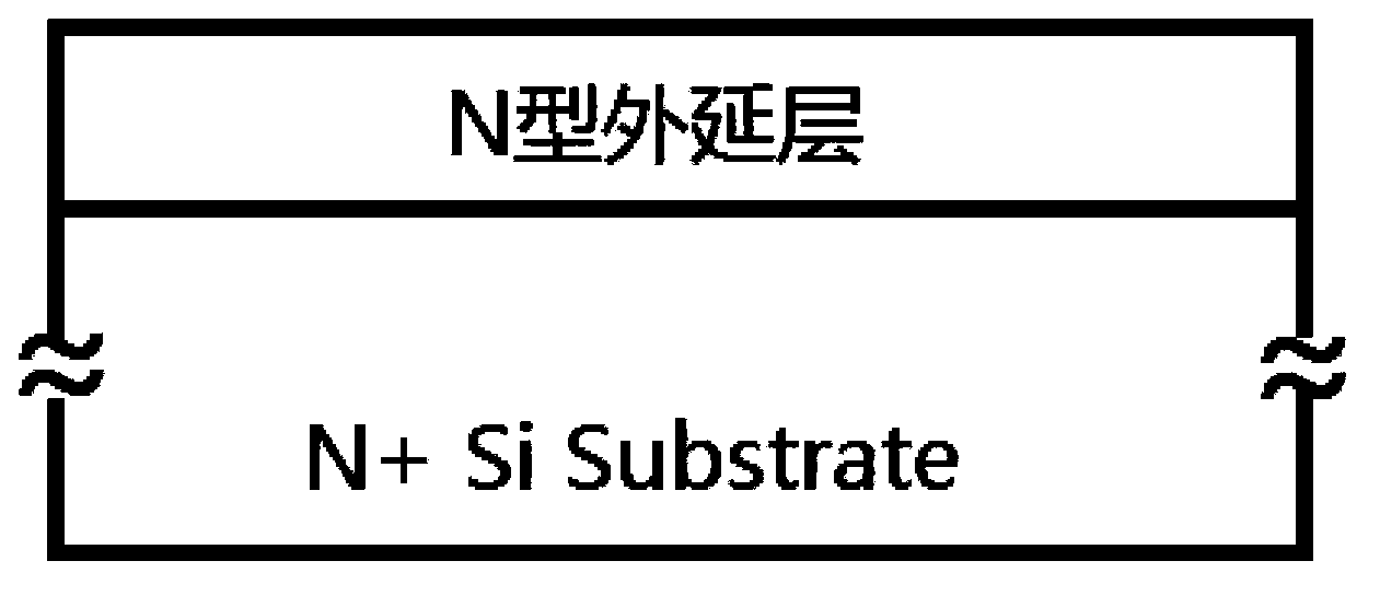
[0029] (1) An N-type silicon epitaxial layer is covered on the N+ type silicon wafer substrate. like figure 1 shown.

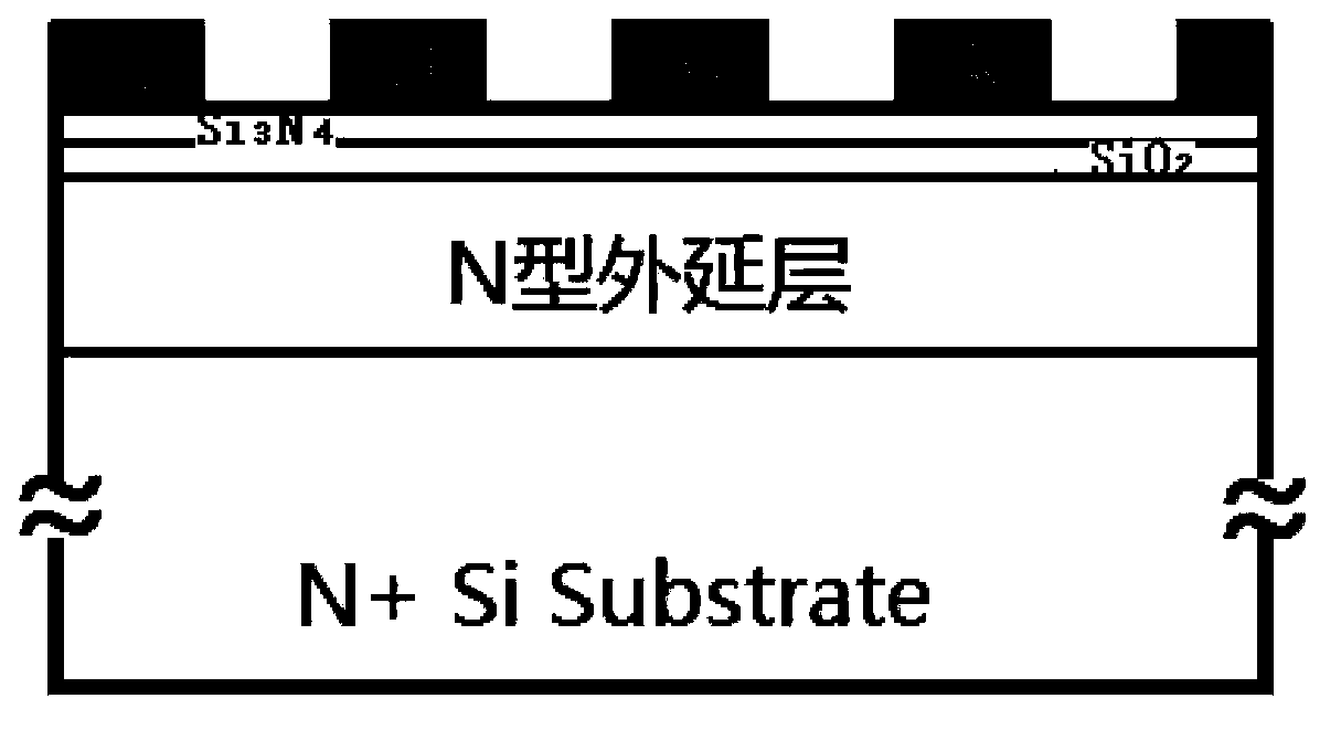
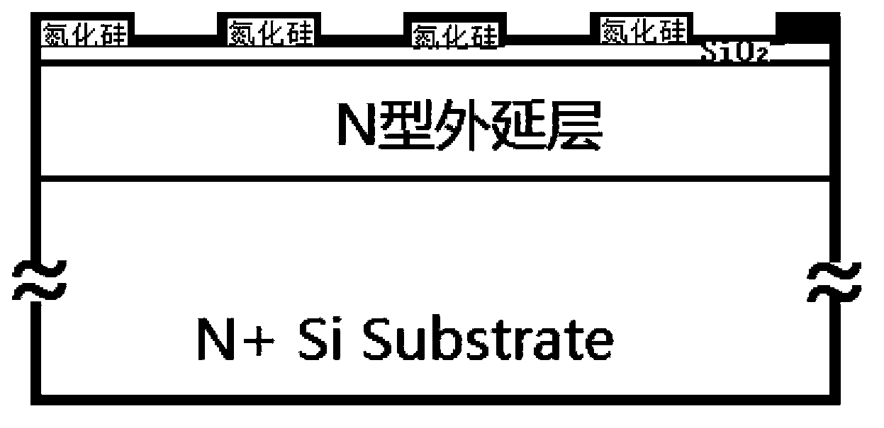
[0030] (2) A thin layer of silicon oxide is first grown on the N-type silicon epitaxial layer, and a layer of silicon nitride is deposited on it; and the thickness of silicon oxide is smaller than that of silicon nitride. In this embodiment, the silicon oxide is SiO 2 , its thickness is about 300 Angstroms; the silicon nitride is Si 3 N 4 , and its thickness is about 2000 Angstroms.

[0031] (3) A plurality of block photoresist regions are formed on the surface of the silicon nitride layer by photolithography, and these block photoresist regions are independently distributed and cover the surface of the silicon nitride layer. like fi...

Embodiment 2

[0043] In Embodiment 2, the N-type and P-type of Embodiment 1 can be exchanged to obtain a barrier junction Schottky diode with P+ type substrate, P-type epitaxial layer and N-type ion implantation, such as Figure 10 shown. which is

[0044]A method for manufacturing a junction barrier Schottky diode using a silicon selective oxidation technique, comprising a crystal generating step and a packaging step, wherein the crystal generating step includes:

[0045] (1) Cover a P-type silicon epitaxial layer on the P+ type silicon wafer substrate; figure 1 shown.

[0046] (2) A thin layer of silicon oxide is first grown on the P-type silicon epitaxial layer, and then a layer of silicon nitride is deposited on it; and the thickness of silicon oxide is smaller than that of silicon nitride. In this embodiment, the silicon oxide is SiO 2 , its thickness is about 300A; the silicon nitride is Si 3 N 4 , and its thickness is about 2000A. The above 1A=10 -4 u.

[0047] (3) A plural...


PUM


Abstract

The invention discloses a method for manufacturing a junction barrier schottky diode through selective oxidation of silicon. As the formation of LOCOS (local oxidation of silicon) monox is adopted, the scope of diffusion of an injected foreign ion is effectively limited within an LOCOS monox area to effectively reduce the scope of lateral (horizontal) diffusion of a P area or an N area of a PN junction, a schottky interface occupied by the lateral diffusion of the P area or the N area is reduced, and the area of the schottky interface is sufficiently utilized. Moreover, the effectively schottky barrier interface is bent into a curve to increase the conductive area and compensate the area occupied by an abnormal-shape island, and the forward-direction electrifying function and the efficiency of the junction barrier schottky diode are improved.

Description

technical field [0001] The invention relates to the design field of diode manufacturing, and specifically relates to a method for manufacturing junction barrier Schottky diodes using silicon selective oxidation technology. Background technique [0002] Schottky diodes are low-power, high-current, ultra-high-speed semiconductor devices that have come out in recent years. Its reverse recovery time is extremely short (can be as small as a few nanoseconds), the forward voltage drop is only about 0.4V, and the rectification current can reach several thousand milliamperes. These excellent characteristics are unmatched by fast recovery diodes. Schottky diodes are made using the principle of metal-semiconductor junctions formed by metal-semiconductor contacts, and are also known as metal-semiconductor (contact) diodes or surface barrier diodes. [0003] Common Schottky diodes have a Schottky barrier interface between the surface metal and the silicon layer. This interface can con...

Claims


Application Information

Patent Timeline
IPC IPC(8): H01L21/329H01L29/872
CPCH01L21/76202H01L29/66143H01L29/872
Inventor 关仕汉李勇昌彭顺刚邹锋王常毅
Owner 桂林斯壮桂微电子有限责任公司
Why Eureka
Try Eureka