How to make a mos transistor

A technology of a MOS transistor and a manufacturing method, which is applied to the manufacturing field of MOS transistors, can solve problems such as poor performance of PMOS transistors, and achieve the effects of easy removal steps and improved performance.

Active Publication Date: 2016-12-21
SEMICON MFG INT (SHANGHAI) CORP
View PDF5 Cites 0 Cited by
  • Summary
  • Abstract
  • Description
  • Claims
  • Application Information

AI Technical Summary

Problems solved by technology

[0005] The technical problem to be solved by the present invention is that the performance of the PMOS transistor formed by the prior art is not good

Method used


Image

  • How to make a mos transistor
  • How to make a mos transistor
  • How to make a mos transistor

Examples


Embodiment Construction

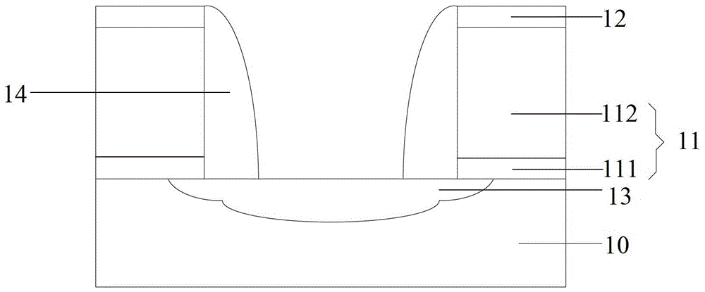
[0040] After research, the inventor found that the reasons for the poor performance of PMOS transistors are:

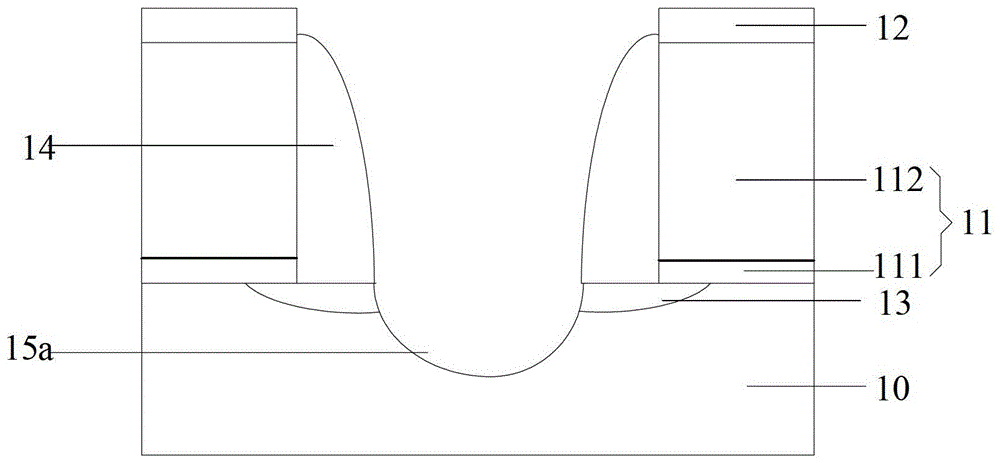
[0041] Please refer to figure 2 The method for forming the sigma-shaped groove includes: using the dummy gate structure 11 and the sidewall 14 as a mask, etching the substrate 10 to form bowl-shaped grooves 15 a in the substrate 10 on both sides of the dummy gate structure 11 . The bowl-shaped groove 15a is formed by using anisotropic dry etching to form rectangular grooves in the substrate 10 on both sides of the dummy gate structure 11, and then using isotropic dry etching to etch the formed grooves. The above-mentioned rectangular groove forms a bowl-shaped groove 15a. The aforementioned anisotropic dry etching and isotropic dry etching cause the first damage to the sidewall 14 , so that the height of the sidewall 14 decreases.

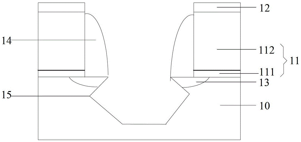
[0042] Please continue to refer figure 2 and image 3 , the bowl-shaped groove 15a is exposed to TMAH (Tetramethyl Ammonium Hydroxi...


PUM


Abstract

A manufacturing method for an MOS (Metal Oxide Semiconductor) transistor is characterized in that a substrate is provided, a dummy gate structure is formed on the substrate and includes gate dielectric layers and dummy gate electrodes located on the gate dielectric layers, and first side walls are formed on the two sides of the dummy gate structure; the substrate is etched with the dummy gate structure and the first side walls serving as masks, and grooves are formed in the substrate on the two sides of the dummy gate structure; the grooves are filled with semi-conductor materials; a sacrificial layer is formed between the first side walls after the semi-conductor materials are formed, and the thickness of the sacrificial layer is smaller than the heights of the first side walls; a dielectric layer is formed to cover the sacrificial layer, the first side walls and the dummy gate structure; the dielectric layer is etched back to form second side walls on the two sides of the dummy gate structure and on the first side walls; the sacrificial layer is removed. The performance of the MOS transistor which is prepared subsequently can be improved through the manufacturing method for the MOS transistor.

Description

technical field [0001] The invention belongs to the field of semiconductor manufacturing, in particular to a method for manufacturing a MOS transistor. Background technique [0002] In the existing manufacturing process of semiconductor devices, since stress can change the energy gap and carrier mobility of silicon materials, it has become an increasingly common means to improve the performance of MOS transistors through stress. Specifically, by properly controlling the stress, the mobility of carriers (electrons in NMOS transistors and holes in PMOS transistors) can be increased, thereby increasing the driving current, thereby greatly improving the performance of MOS transistors. For PMOS transistors, embedded silicon germanium technology (Embedded SiGe Technology) can be used to generate compressive stress in the channel region of the transistor, thereby improving carrier mobility. The so-called embedded silicon germanium technology refers to embedding silicon germanium m...

Claims


Application Information

Patent Timeline
Patent Type & Authority Patents(China)
IPC IPC(8): H01L21/336H01L21/28
CPCH01L21/28132H01L29/66545
Inventor 隋运奇孟晓莹
Owner SEMICON MFG INT (SHANGHAI) CORP
Why Eureka
Try Eureka