Broad band band-pass filter

A technology of band-pass filter and low-pass filter, which is applied in the filter field, can solve the problems of complex design structure and high production cost, and achieve the effect of simple processing, low cost and small size

Active Publication Date: 2014-04-09
GUANGDONG MIKWAVE COMM TECH
View PDF8 Cites 9 Cited by
  • Summary
  • Abstract
  • Description
  • Claims
  • Application Information

AI Technical Summary

Problems solved by technology

However, these high-tech production costs are high, and the design structure is relatively complicated

Method used


Image

  • Broad band band-pass filter
  • Broad band band-pass filter
  • Broad band band-pass filter

Examples


Embodiment 1

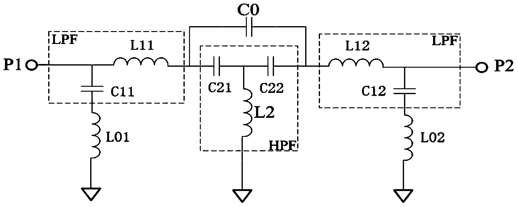
[0031]A broadband bandpass filter, suitable for making in a multi-layer circuit board, consists of a first low-pass filter unit, a high-pass filter unit, and a second low-pass filter unit connected in sequence, and the input port P1 is connected to the first The low-pass filter unit is connected, and the second low-pass filter unit is connected to the output port P2. The circuit has a symmetrical structure, wherein the inductor L11 and the capacitor C11 form the first low-pass filter unit, and one end of the capacitor C11 is connected to the input port P1 and the inductor L11. , the other end is connected to the inductor L01, and the inductor L01 is grounded; one end of the two symmetrical capacitors C21 and C22 is connected in series with the inductor L2 to form a high-pass filter unit, the inductor L2 is grounded, and the two symmetrical capacitors C21 and C22 pass through the capacitor C0 phase coupling; the second low-pass filter unit is composed of inductor L12 and capacit...

Embodiment 2

[0042] (1) The dielectric substrate adopts Rogers RO4003 substrate, the single-layer thickness is 0.5mm, the metal layer material is silver-plated copper-clad, and the processing accuracy is ±0.01mm;

[0043] (2) figure 1 Among them, L11=2.8nH, L12=2.8nH, L2=4.6nH, L01=0.8nH, L02=0.8nH, C11=1.3pF, C12=1.3pF, C21=2.8pF, C22=2.8pF, C01=0.31 pF,C02=0.31pF;

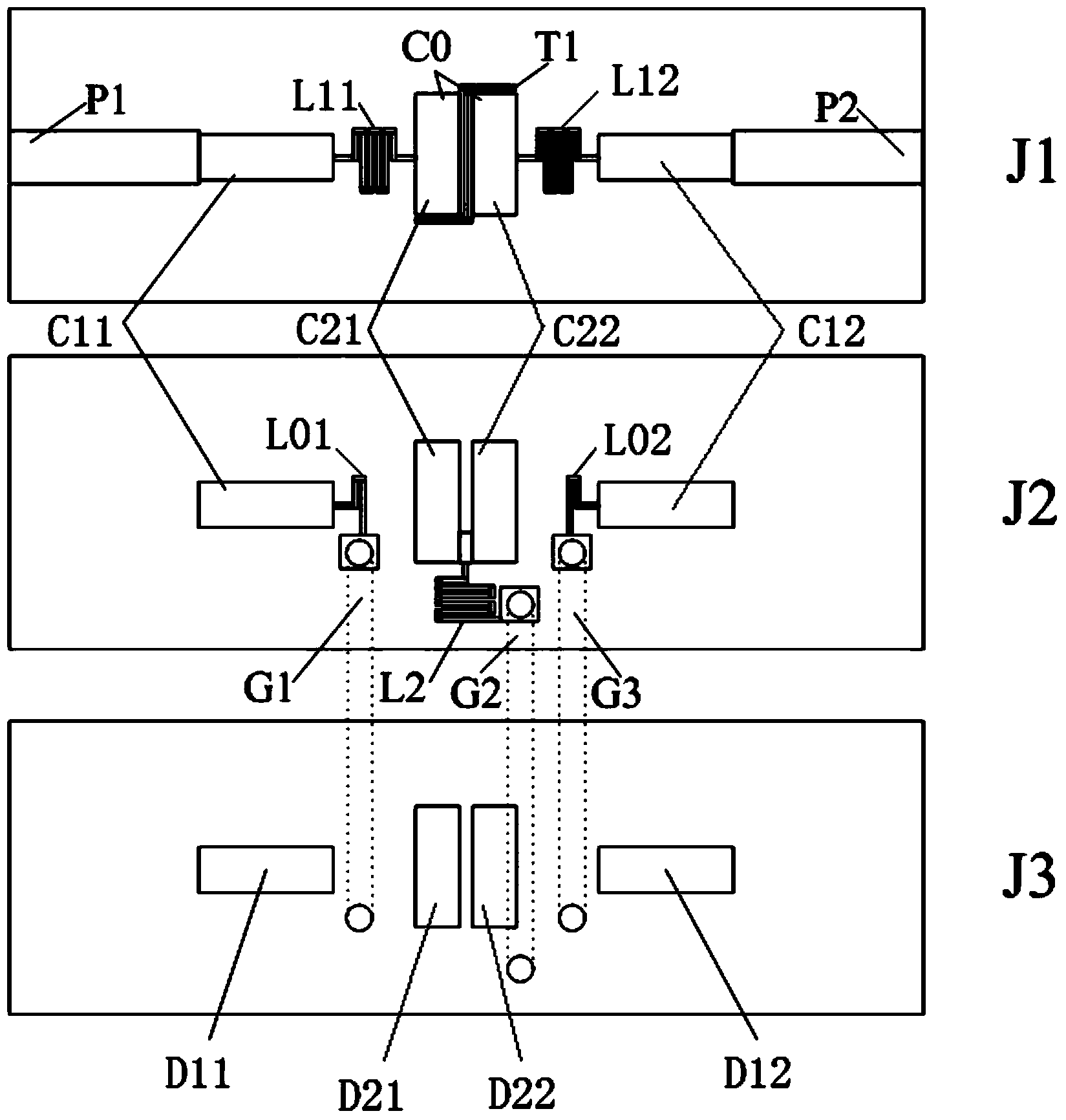
[0044] (3) figure 2 Among them, the first input microstrip transmission line P1 has a line width of 2.3mm and a length of 7.0mm; inductors L11 and L12 have a line width of 0.2mm, a line spacing of 0.1mm, and a length of 16.1mm; the inductor L2 has a line width of 0.2mm, a line spacing of 0.1mm, and a length of 19.1mm; inductor L01, L02 line width 0.2mm, line spacing 0.1mm, length 4.5mm; capacitor C11, C12 line width 2.0mm, length 4.9mm; capacitor C21, C22 line width 2.8mm, length 6.7mm; capacitor C0 line Width 0.2mm, gap 0.1mm, length 2.8mm, the first metal ground via (G1), the second metal ground via (G2), and the third ...


PUM


Abstract

The invention relates to a filter, in particular to a broad band band-pass filter with a multilayer structure. According to the design, a lumped parameter element model of the band-pass filter is achieved by adopting a multilayer micro-strip structure, inductors are designed by using spiral broken lines, capacitors are designed by adopting a flat plate structure, and equivalent resonance circuits are formed by combining the spiral inductors and the flat plate capacitors. The broad band band-pass filter with the multilayer structure is structurally composed of three metal conduction band layers and two transmitting medium layers, wherein the series connection of the two inductors L1 and one coupling capacitor C0 is achieved on the first metal conduction band layer, the two series resonance circuits are connected in parallel on the second metal conduction band layer, the ground connection of three metal via holes is achieved on the third metal conduction band layer, and ground capacitance coupling is removed by digging cracks. Through the combination of the modern technology, the broad band band-pass filter with the multilayer structure is capable of meeting the requirements for miniaturization and broad bands, and has certain simple practicality.

Description

technical field [0001] The invention relates to a filter, in particular to a small-sized broadband band-pass filter with a multi-layer structure. Background technique [0002] In modern communication systems, bandpass filters are widely used as an important component. In the past few years, traditional bandpass filters based on parallel coupled microstrip lines have been extensively studied. As we all know, the size of traditional coupled microstrip filters is very large in both L-band and S-band. With the continuous development of the communication industry, people's requirements for miniaturization and broadband are getting higher and higher. Research extensively. However, these high-tech processes have high production costs and complex design structures. This design is a multi-layer structure bandpass filter based on microwave PCB design, which has the advantages of small size, wide bandwidth, simple structure and low cost. Contents of the invention [0003] The obj...

Claims


Application Information

Patent Timeline
Patent Type & Authority Applications(China)
IPC IPC(8): H01P1/203
Inventor 程勇黄正伟朱洪波徐燕
Owner GUANGDONG MIKWAVE COMM TECH
Why Eureka
Try Eureka