Wafer edge protection ring and method for reducing particles at wafer edge

An edge protection and protection ring technology, which is applied in the manufacture of discharge tubes, electrical components, semiconductors/solid-state devices, etc., can solve problems such as damage to chip quality, and achieve the effects of easy control, quality assurance, and particle reduction

Active Publication Date: 2014-04-16
ADVANCED MICRO FAB EQUIP INC CHINA
View PDF7 Cites 35 Cited by
  • Summary
  • Abstract
  • Description
  • Claims
  • Application Information

AI Technical Summary

Problems solved by technology

[0005] However, it is precisely because the helium flow rate is increased after the high-voltage direct current is turned off during the wafer release process that the process reaction by-products containing polymers are blown by the helium gas flow to the edge of the wafer to form particles, thereby damaging the The quality of chips at the edge of the wafer

Method used


Image

  • Wafer edge protection ring and method for reducing particles at wafer edge
  • Wafer edge protection ring and method for reducing particles at wafer edge
  • Wafer edge protection ring and method for reducing particles at wafer edge

Examples


Embodiment 1

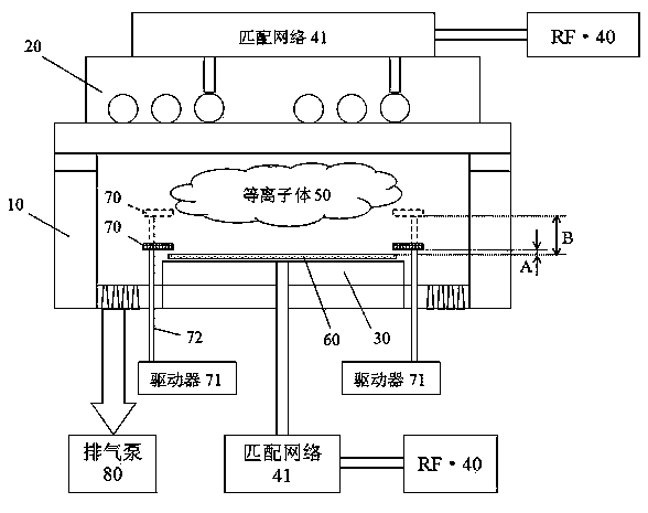
[0033] Cooperate see figure 1 , figure 2 As shown, the first embodiment of the present invention provides a wafer edge protection ring (hereinafter referred to as the protection ring 70 for short), which is located in the reaction chamber 10 of the plasma processing apparatus. The protection ring 70 covers the edge of the wafer 60 .

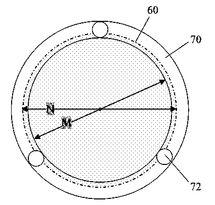
[0034] The inner diameter M of the protective ring 70 is equal to or slightly smaller than the diameter N of the wafer 60: for example, if the diameter of the wafer 60 is 200mm, the inner diameter of the protective ring 70 can be 196mm~200mm; if the diameter of the wafer 60 is 300mm Yes, the inner diameter of the protection ring 70 may be 294mm~300mm.

[0035] A driver 71 (for example, including a motor, a cylinder, etc.) is provided on the atmospheric side of the reaction chamber 10 . The driver 71 can connect the protective ring 70 through several connecting rods 72 penetrating into the reaction chamber 10 , so as to control the rising or f...

Embodiment 2

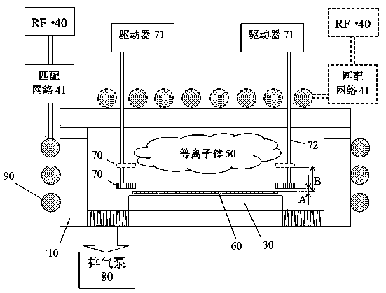
[0040] Such as image 3 As shown, the protective ring 70 provided in the second embodiment of the present invention is characterized in that the driver 71 of the protective ring 70 is located above the top of the plasma processor reaction chamber 10 and is on the atmospheric pressure side. A plurality of connecting rods 72 penetrate into the reaction chamber 10 from top to bottom to connect the protection ring 70 , and the protection ring 70 is suspended above the wafer 60 and covers the edge of the wafer 60 . Under the action of the driver 71, the protection ring 70 can be lowered to the first state, so that there is a first gap A between the bottom surface of the protection ring 70 and the top surface of the wafer 60 (edge ​​position); it is also possible to make the protection ring 70 pulled up to the second state ( image 3 Indicated by a dotted line), the distance between the bottom surface of the guard ring 70 and the top surface of the wafer 60 (edge ​​position) is inc...

Embodiment 3

[0044] The present invention also provides another structure of the protective ring, which can be applied to Embodiment 1 or 2. The characteristic is that the protective ring is composed of equal or non-equal segments of arcs, and the driver controls these arc segments to spread out or gather in the horizontal direction through corresponding connecting rods instead of making them lift up and down. . The circular arc segments can be supported from below or suspended from above by means of vertically arranged connecting rods, and can also be driven by means of horizontally arranged connecting rods.

[0045] Such as Figure 4 As shown, for example, in a protective ring provided, there are two semi-circular arc segments 70-1, 70-2, and the two are in a state of gathering during wafer processing, so as to form a complete cover on the A ring structure at the edge of the wafer to hold process reaction by-products including polymers. While releasing the wafer, the two semicircle ar...


PUM


Abstract

The invention relates to a wafer edge protection ring and a method for reducing particles at a wafer edge. The protection ring is located in a reaction cavity of a plasma processing device, the protection ring can cover the wafer edge in the process that a wafer is processed so that processing byproducts including polymers can be borne, and the protection ring can move in the process that the wafer is released and take the collected polymers off the wafer. The wafer edge protection ring is simple in structure, convenient to control and capable of effectively reducing the particles at the wafer edge and guarantees quality of a chip on the wafer edge.

Description

technical field [0001] The invention relates to a plasma processing device in the field of semiconductor manufacturing, in particular to a wafer edge protection ring and a method for reducing wafer edge particles. Background technique [0002] Currently, for example, in some plasma processing devices used for etching or TSV (Through Silicon Via) processes, a processing table is usually provided at the bottom of the reaction chamber for carrying a wafer placed thereon. During the process, the reaction gas is introduced into the reaction chamber through the upper electrode and maintained at the set pressure value under the action of the pressure controller. A radio frequency power supply (for example, 13.56MHz, 3000W) is connected to the processing table or the upper electrode through a matching network, and is used to form a radio frequency field between the processing table and the upper electrode to excite the reactive gas into a plasma state, so as to facilitate the use of...

Claims


Application Information

Patent Timeline
Patent Type & Authority Applications(China)
IPC IPC(8): H01J37/32H01L21/683
Inventor 周旭升徐朝阳倪图强许颂临
Owner ADVANCED MICRO FAB EQUIP INC CHINA
Why Eureka
Try Eureka