Junction field effect transistor and manufacturing method thereof

A technology of field effect transistors and surface junctions, applied in the manufacture of surface junction field effect transistors, in the field of surface junction field effect transistors, can solve problems such as increased process costs, achieve reduced doping concentration, small pinch-off voltage, and large The effect of channel current

Inactive Publication Date: 2014-04-16
SHANGHAI HUAHONG GRACE SEMICON MFG CORP
View PDF3 Cites 2 Cited by
  • Summary
  • Abstract
  • Description
  • Claims
  • Application Information

AI Technical Summary

Problems solved by technology

However, the disadvantage of the existing third type of JFET is that it is necessary to add an extra layer of mask on the stand

Method used


Image

  • Junction field effect transistor and manufacturing method thereof
  • Junction field effect transistor and manufacturing method thereof
  • Junction field effect transistor and manufacturing method thereof

Examples


Example Embodiment

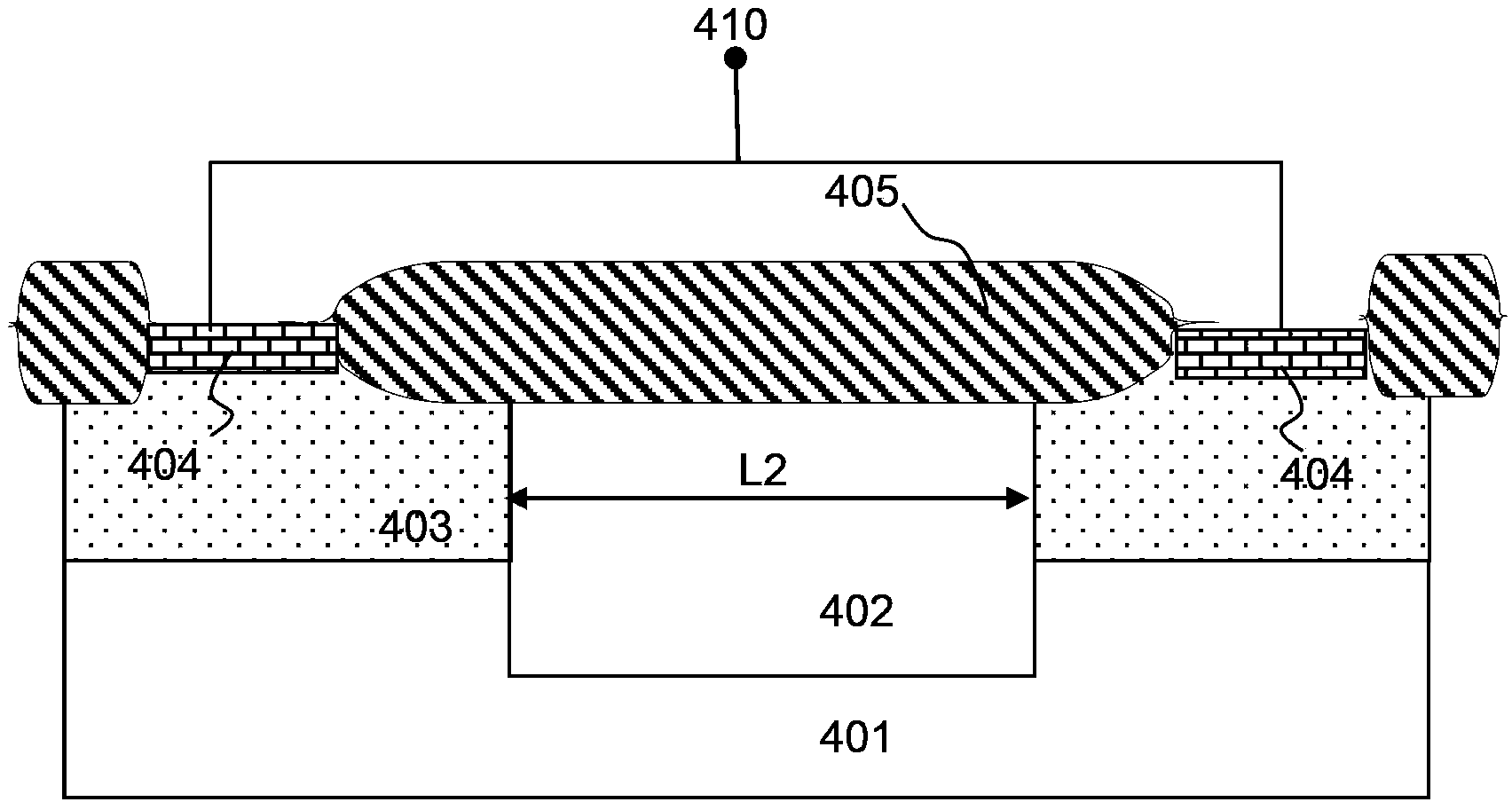
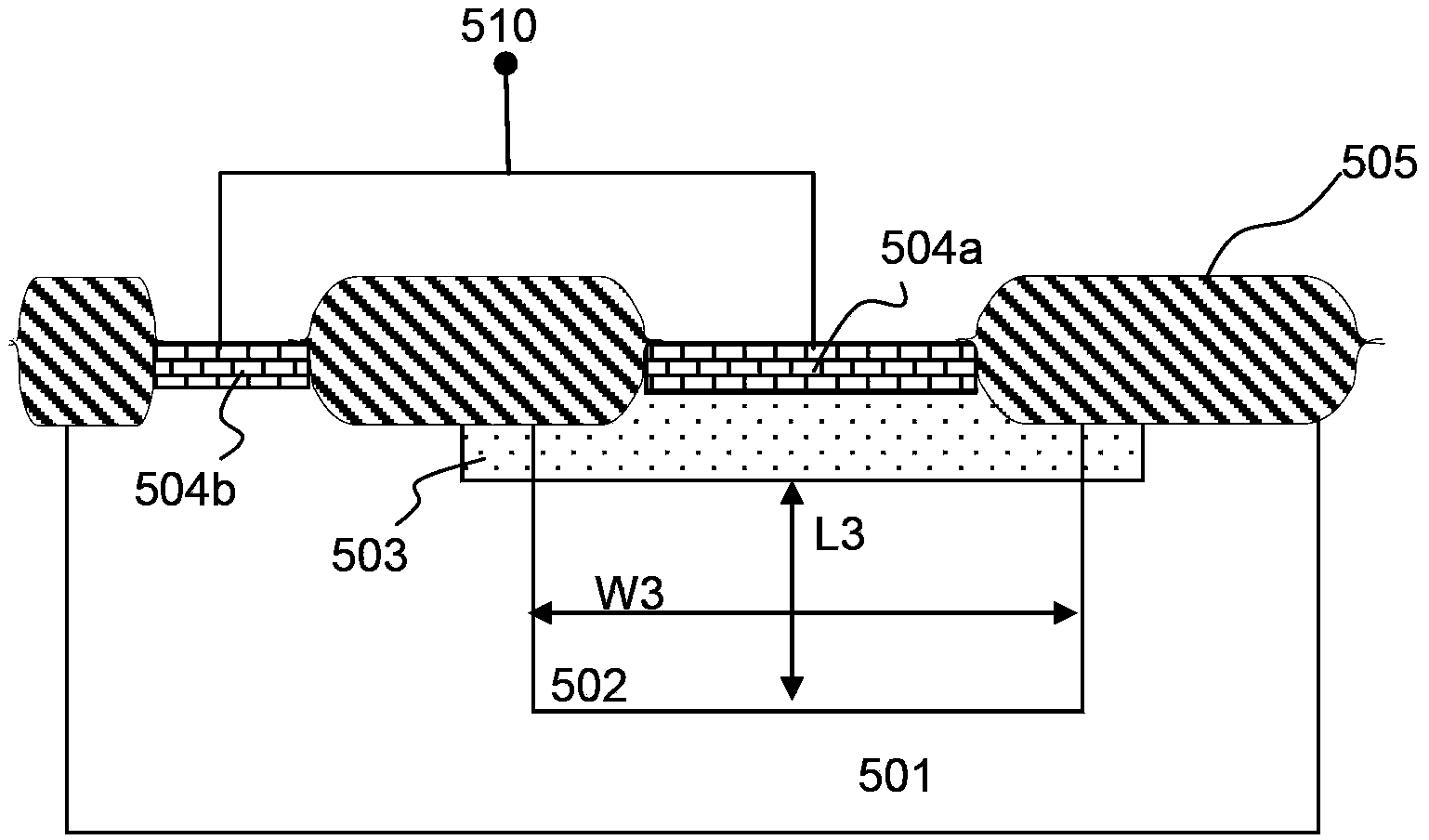
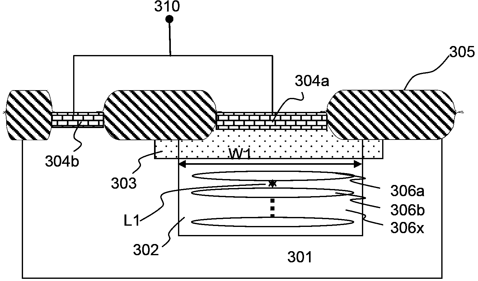
[0049] Such as Figure 4A Shown is a schematic top view of a junction field effect transistor according to an embodiment of the present invention; Figure 4B Shown, is Figure 4A Schematic diagram of the section along the line AA; Figure 4C Shown, is Figure 4A Schematic diagram of the section along the line BB. The junction field effect transistor in the embodiment of the present invention takes a device whose channel conductivity type is N-type carrier as an example. The JFET in the embodiment of the present invention includes:

[0050] Two N-type wells 102a and 102b are formed on a P-type semiconductor substrate such as a silicon substrate 101. Such as Figure 4A As shown, the two N-type wells are both rectangular, the adjacent width sides of the two N-type wells 102a and 102b are the same size, that is, the width W1, and the two N-type wells 102a and 102b are adjacent The two ends of the width side are aligned and separated by the distance S1.

[0051] The region between the...


PUM


Abstract

The invention discloses a junction field effect transistor. A channel region is arranged between two adjacent same-doped well regions, the channel region is doped through diffusion of the two adjacent well regions, and well regions with the opposite doping types are arranged above the channel region and used for longitudinal depleting the channel region. According to the junction field effect transistor, the doping concentration of the channel region can be reduced, the pinch-off voltage of the channel region is lowered, and thus the pinch-off voltage of the channel region can be adjusted, a small pinch-off voltage is obtained and extra cost does not need to be added. The width requirement of the channel region can be met just by adjusting the widths of the two adjacent same-doped well regions on the two sides of the channel region, and thus the channel current of the device can be adjusted; moreover, the channel current can be enlarged easily, and thus a large channel current is obtained. The invention further discloses a manufacturing method of the junction field effect transistor.

Description

technical field [0001] The invention relates to the field of semiconductor integrated circuit manufacturing, in particular to a junction field effect transistor (JFET). The invention also relates to a method for manufacturing the junction field effect transistor. Background technique [0002] At present, the commonly used JFETs are divided into two types: horizontal pinch off and vertical pinch off. [0003] Such as figure 1 As shown, it is a structural schematic diagram of the first existing surface junction field effect transistor; the existing first JFET is a lateral pinch-off JFET, taking the N-type structure as an example, the existing first JFET includes: [0004] The N-type well 402 is formed on the P-type silicon substrate 401, and the N-type well 402 is used as a channel region. [0005] Two P-type wells 403 are formed on both sides of the N-type well 402. The two P-type wells 403 are used to laterally deplete the N-type well 402 from both sides of the N-type wel...

Claims


Application Information

Patent Timeline
IPC IPC(8): H01L29/808H01L29/10H01L21/337
CPCH01L29/808H01L29/1033H01L29/66901
Inventor 金锋苗彬彬
Owner SHANGHAI HUAHONG GRACE SEMICON MFG CORP
Why Eureka
Try Eureka